The Essential List of Electronic Materials
1 Introduction
Electronic materials play an utterly crucial role in the rapidly evolving landscape of modern electronics. They are the fundamental building blocks that underpin the functionality and performance of a vast array of electronic devices, ranging from ubiquitous smartphones and laptops to highly sophisticated aerospace and medical equipment. These materials determine the electrical, thermal, mechanical, and optical properties of the devices, thereby dictating their capabilities and limitations.
The development and innovation of electronic materials have been the driving force behind the continuous progress of the electronics industry. With the ever-increasing demand for smaller, faster, more energy-efficient, and highly reliable electronic products, the search for and utilization of advanced electronic materials has become more urgent than ever. In the following sections, we will embark on an in-depth exploration of several key electronic materials, including silicon, silicon carbide, germanium, gallium compounds, carbon-based materials, conductive and insulating materials, and magnetic materials. By understanding their unique properties, manufacturing processes, and diverse applications, we can gain a comprehensive perspective on the significance and potential of these materials in shaping the future of electronics.
2 Silicon and Related Materials
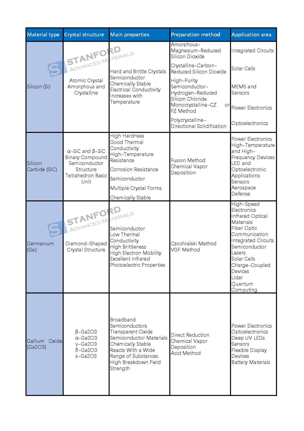
Silicon (Si), atomic number 14, is a hard and brittle crystalline, quasi-metallic, and semiconducting material with both amorphous and crystalline forms, and is abundant in the earth's crust. Silicon has four valence electrons in the outermost layer of the atom and is chemically relatively stable, making it difficult to react with other substances at room temperature. As a semiconductor material, the electrical conductivity of silicon increases with increasing temperature and is widely used in various electronic devices.
In the extraction and production of silicon, amorphous silicon is usually obtained by reducing silicon dioxide with magnesium. In contrast, crystalline silicon is produced in an electric furnace by reducing silicon dioxide with carbon. High-purity semiconductor silicon can be prepared by hydrogen reduction of silicon chloride. Monocrystalline silicon is usually made by the Czochralski method or zone fusion (FZ method), while polycrystalline silicon is grown by directional solidification.
Silicon has a wide range of applications in the electronics industry, especially as a chip substrate in integrated circuits, where it is an ideal material for manufacturing transistors. In addition, monocrystalline silicon, polycrystalline silicon, and thin silicon films are widely used in solar cells. In the field of microelectromechanical systems (MEMS) and sensors, silicon is used in the manufacture of accelerometers, gyroscopes, and pressure sensors. Silicon is also used in power electronics to make power semiconductor devices such as MOSFETs (Metal Oxide Semiconductor Field Effect Transistors) and IGBTs (Insulated Gate Bipolar Transistors). In the field of optoelectronics, silicon photodiodes are widely used in optical communication systems.
The advantages of silicon are its abundant reserves, sustainable utilization, controlled purity, and low cost, however, there are some drawbacks such as poor high-temperature performance and narrow bandgap, which limits its use in high-speed and high-frequency applications.
Read more: Essential Electronic Materials: Part 1 - Silicon
Fig.1 Silicon Products
3 Silicon Carbide (SiC)
Silicon carbide (SiC) is a broadband semiconductor material with high hardness, good thermal conductivity, high temperature, and corrosion resistance. Its chemical formula is SiC, and there are various crystal structures, the most common are α-SiC and β-SiC. Industrially produced silicon carbide shows different colors due to different impurities. Through doping techniques, it is possible to change its energy level structure and thus adjust its electronic and other physical properties.
The main manufacturing processes for silicon carbide include fusion and chemical vapor deposition (CVD). The fusion method forms silicon carbide by mixing and melting silicon and graphite at high temperatures and then cooling them. Chemical vapor deposition deposits SiC on the substrate surface through a gas-phase chemical reaction and is commonly used to produce high-quality thin film materials.
Silicon carbide is used in a wide variety of applications. In power electronics, SiC is used in power conversion devices to improve the efficiency of electric vehicles and renewable energy systems. In high-temperature, high-frequency devices, SiC is suitable for 5G base stations and military electronics because of its ability to maintain stable operation under extreme conditions. In addition, SiC plays a role in LED and optoelectronics applications, initially used in blue LEDs and now used for light detection at specific wavelengths. In the field of sensors, SiC is commonly used for detection in high-temperature, high-pressure, and radiation environments because of its reliability in extreme environments. The high reliability of SiC also makes it popular for aerospace and defense applications.
The advantage of silicon carbide is its excellent high-temperature, high-pressure, and high-frequency high-power performance, which provides high energy conversion efficiency. However, it also has some drawbacks, such as higher cost, complex fabrication process, and the reliability of its devices still needs to be further improved.
Read more: Essential Electronic Materials: Part 2 - Silicon Carbide
Fig. 2 Silicon Carbide Chip
4 Germanium and Related Materials
Germanium (Ge) is a semiconductor element with an atomic number of 32 and a crystal structure similar to that of diamond. Germanium has a density of 5.323 g/cm³, a melting point of 937.4°C, and a boiling point of 2833°C. As a semiconductor material, germanium has a bandgap of 0.66 eV, and exhibits good electrical conductivity at low temperatures, with particular excellence in infrared optoelectronic properties. However, germanium has a low thermal conductivity and a high degree of brittleness, properties that limit its performance in certain applications.
The manufacturing process for germanium is typically used to prepare single-crystal germanium by the straight drawing method (Czochralski method) and the vertical gradient solidification method (VGF method). In the straight drawing method, molten germanium liquid is pulled through crystallization to obtain single crystals, while the vertical gradient solidification method guides the growth of crystals by controlling the temperature gradient to ensure their quality and purity.
Germanium has important applications in several fields. In high-speed electronics, germanium is used in high-frequency transistors and wireless communication devices because it has a high electron mobility that supports high-speed signal processing. In addition, germanium is an important infrared optical material and is widely used in infrared detectors and imaging systems. Due to its good optoelectronic properties, germanium is also doped into optical fibers to improve the performance of optical fibers and is used in optical communications, photovoltaic conversion devices, and solar cells. In integrated circuits, germanium is combined with silicon to form alloys that further enhance performance. Germanium is also used in the fabrication of semiconductor lasers, charge-coupled devices (CCDs), and LIDAR, and has potential applications in quantum computing and quantum technology.
The main advantages of germanium include high electron mobility, a low bandgap, high infrared transmittance, and good compatibility with silicon, which makes it well-suited for use in areas such as high-efficiency solar cells and quantum computing. However, it also has significant drawbacks, including low thermal conductivity, high price, difficulty in crystal growth, and restricted industrial production scale, which poses a challenge to the widespread use of germanium.
Read more: Essential Electronic Materials: Part 3 - Germanium
Fig. 3 Germanium for Chip Manufacturing
5 Gallium Compounds
Gallium oxide (Ga2O3): wide-band semiconductor with various crystal structures, such as β-Ga2O3, α-Ga2O3, and so on. It is chemically stable and can react with a variety of substances. It can be prepared by direct reduction method, chemical vapor deposition method, and acid method. Widely used in power electronics, optoelectronic devices (such as ultraviolet detectors, and deep-ultraviolet LEDs), sensors, and other fields, the market scale is growing rapidly, and the industry chain is gradually improving.
Gallium arsenide (GaAs): black gray solid, melting point 1238 ° C, is an important Ⅲ-V compound semiconductor, with cubic crystal structure, excellent electronic properties, low noise, and high breakdown voltage. It is mainly prepared by Vertical Gradient Solidification (VGF), Liquid Encapsulated Direct Drawing (LEC), Horizontal Bridgman (HB), Chemical Vapor Deposition (CVD), and other methods. It is widely used in the microwave, optoelectronics, communications, solar cells, microelectronics, and other fields.
Gallium Nitride (GaN): The crystal structure consists of a lattice of gallium and nitrogen atoms with a wide direct band gap, high hardness, high thermal conductivity, good chemical stability, and other characteristics. It is grown by chemical vapor deposition reactions, such as MOCVD and other methods. Widely used in new electronic devices (e.g., high-power high-frequency devices), optoelectronic devices (e.g., short-wavelength light-emitting devices), sensors, and other fields, which promotes the related technological progress.
Read more: Essential Electronic Materials: Part 4 - Gallium Compounds
Fig. 4 Gallium Oxide Semiconductor Materials
6 Carbon-Based Materials
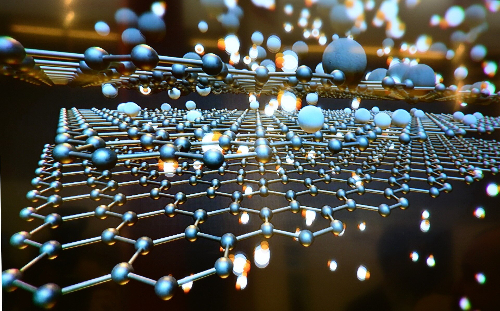
Graphene: A monolayer structure in which carbon atoms are hybridized with sp² to form a hexagonal honeycomb lattice, with excellent optical, electrical, and mechanical properties. With high electron mobility, it has potential applications in integrated circuits, field effect transistors, organic light-emitting diodes, chemical sensors, and optoelectronic devices.
Carbon nanotubes (CNTs): Arranged by carbon atoms into a coaxial circular tube structure, with unique electrical properties, divided into metallic and semiconducting carbon nanotubes. They can be used to manufacture high-performance field effect transistors, electronic sensors, solar cells, etc. to improve the performance of related devices.
Fullerenes (Fullerenes): are hollow molecules composed of carbon atoms, such as C60, etc., with special optical, electrical, and chemical properties. It has important applications in capacitors, conductive adhesives, optoelectronic applications, etc., and can improve electrode conductivity and energy storage density, etc.
Read more: Essential Electronic Materials: Part 5 - Carbon-Based Materials
Fig. 5 Graphene
7 Conductive and Insulating Materials
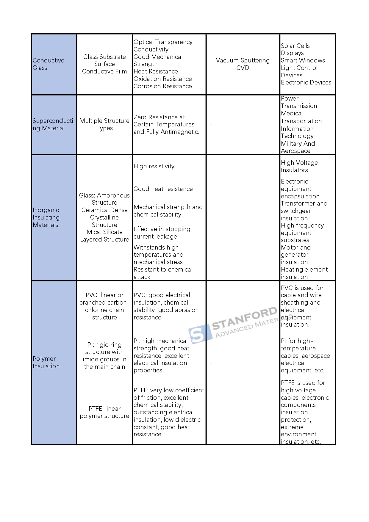
Conductive materials: metals and alloys due to the metal atom's outer electron easy to form free electrons and conductive, with high electrical conductivity, good thermal conductivity, and mechanical strength, such as copper, silver, aluminum and its alloys in the wire and cable, electronic equipment, and other fields are widely used; conductive ceramics conduct electricity through ionic migration or electron transport, both high temperature and corrosion resistance, such as indium tin oxide (ITO) for touch screens, etc.; conductive glass by the glass substrate and surface conductive film composition, with transparent conductivity for solar cells, display screens, etc.; superconducting materials at specific temperatures with zero resistance and completely anti-magnetic. Conductive glass consists of the glass substrate and surface conductive film, with transparent conductivity, used in solar cells, displays, etc.; superconducting materials at a specific temperature resistance is zero and have a completely antimagnetic, divided into low-temperature superconductivity, high-temperature superconductivity and other types of superconductivity in power transmission, medical, transportation, information technology, and other fields are widely used.
Insulating materials: inorganic insulating materials such as glass, ceramics, mica, etc., with high resistivity, good heat resistance, mechanical strength and chemical stability, used for electrical insulation, such as glass for high-voltage insulators, ceramics used for transformer insulation, etc.; polymer insulating materials such as PVC, polyimide (PI), polytetrafluoroethylene (PTFE), etc., with different insulating properties and characteristics. They are suitable for different electronic equipment and environments.
Read more: Essential Electronic Materials: Part 6 - Conductive and Insulating Materials
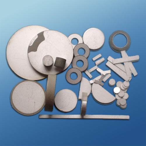
Fig. 6 Electronic Ceramic Materials
8 Magnetic Materials
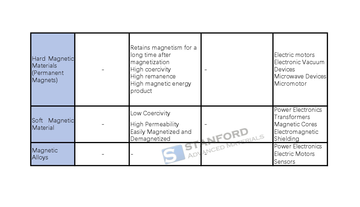
Hard magnetic materials (permanent magnets): such as alnico alloys, titanium-cobalt alloys, rare-earth cobalt permanent magnets, etc., which can maintain magnetism for a long time after magnetization and have high coercivity, high remanence, and high magnetic energy product, and are used in electric motors, electronic vacuum devices, and microwave devices.
Soft magnetic materials: such as silicon steel soft magnets, soft magnetic ferrite, etc., low coercivity, high permeability, easy to magnetize and demagnetize, widely used in transformers, motors, inductors, electromagnetic shielding, and other electronic equipment, can reduce energy loss, improve efficiency.
Magnetic alloys: composed of iron and other metal elements, they are divided into soft magnetic alloys and hard magnetic alloys, which are widely used in the fields of electronics, communications, energy, etc., such as neodymium-iron-boron (NdFeB) used in electric motors, etc., and aluminum-nickel-cobalt alloys used in high-temperature special environments. The properties of magnetic materials such as permeability, saturation flux density, coercivity, etc. are critical to the performance of electronic devices and play a key role in power supplies, transformers, data storage, motors, sensors, wireless communications, and other equipment.
Read more: Essential Electronic Materials: Part 7 - Magnetic Materials
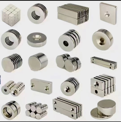
Fig. 7 NdFeB Magnets
9 Conclusion
In conclusion, electronic materials are the bedrock of modern electronics. Silicon has been prominent, yet materials like silicon carbide and gallium compounds are emerging. Carbon-based materials bring new opportunities. Conductive, insulating, and magnetic materials are also vital. The development trends point towards better performance and reliability. Efforts are made to improve materials like silicon carbide and gallium nitride. Research on carbon-based materials focuses on synthesis and integration. Continuous research and innovation are crucial. They meet existing demands and enable new technologies. Exploring and optimizing materials is essential for the electronics industry's progress.
Stanford Advanced Materials (SAM) is a key provider of high-quality electronic materials, supporting these critical applications with reliable material solutions.
