Essential Electronic Materials: Part 1 - Silicon
1 Introduction
Silicon, a fundamental material in modern electronics, is essential in applications from integrated circuits to solar cells. As a tetravalent quasi-metal and semiconductor, silicon's structure and properties make it invaluable in electronic devices. Its abundance, affordability, and highly tunable purity have secured its role as the foundational material in the industry. This article discusses silicon’s basic properties, extraction and production processes, and applications, along with its advantages and limitations, providing an overview of why silicon continues to be the cornerstone of electronic material science.
2 Basic Properties of Silicon
Silicon is a chemical element with the chemical symbol Si, atomic number 14, and relative atomic mass 28.0855. It is a hard, brittle crystalline solid, a tetravalent quasi-metal, and a semiconductor. It is a hard, brittle crystalline solid, a tetravalent quasi-metal, and a semiconductor. It has two isomers, amorphous and crystalline silicon, and belongs to the third period of the periodic table of the elements, the IVA group of metalloid elements. Crystalline silicon is gray-black, density of 2.32-2.34 g/cm3, a melting point of 1410 ℃, and a boiling point of 2355 ℃, crystalline silicon belongs to the atomic crystal. Insoluble in water, nitric acid, and hydrochloric acid, soluble in hydrofluoric acid and lye. Hard and has a metallic luster.
Silicon is also a common element in nature, usually in the form of complex silicates or silica, widely present in rocks, gravel, and dust. Silicon is the eighth most abundant in the universe. It is widely distributed in dust, sand grains, planetesimals, and planets as silica (silicates) or silicates. More than 90% of the Earth's crust is composed of silicate minerals, making silicon the second most abundant element in the Earth's crust (about 28% by mass), after oxygen.
The silicon atom is located in the main group IV of the periodic table; it has an atomic number of 14 and 14 electrons outside its nucleus. Electrons outside the nucleus, according to the energy level from low silicon atom to high, from inside to outside, layers around. The first layer of electrons outside the nucleus of the silicon atom has 2 electrons, and the second layer has 8 electrons, reaching a stable state. The outermost layer has 4 valence electrons, which play a leading role in the conductivity of the silicon atom.
Because the silicon atom has such a structure, there are some of its special properties: the outermost 4 valence electrons so that the silicon atoms with each other to covalent bonding, silicon has a high melting point and density; chemical properties are more stable, room temperature is difficult to react with other substances (except hydrogen fluoride and lye); silicon crystals in the concentration of free electrons are very low, can be conductive, but conductivity is not as good as the metal, with the increase in temperature and increased, with semiconductor properties.
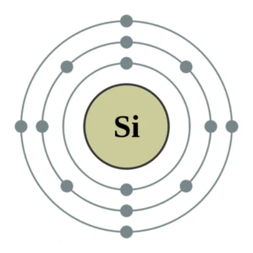
Fig. 1 Atomic Structure of Silicon
3 Silicon extraction and production process
3.1 Preparation of Amorphous and Crystalline Silicon
Amorphous silica can be produced by the reduction of silica by magnesium. In the laboratory, magnesium powder can be used to reduce powdered silica under red heat, and the resulting magnesium oxide and magnesium powder are washed away with dilute acid, and then hydrofluoric acid is used to wash away the silica that has not been acted upon, that is, the monomorphic silica is obtained. This method of production is not pure enough amorphous silicon, for the brownish-black powder.
Crystalline silicon can be produced by reducing silicon dioxide with carbon in an electric furnace. Silicon is produced industrially by reducing silica (>99% SiO2) in an electric arc furnace. The reducing agents used are petroleum coke and charcoal, among others. When using a direct current arc furnace, can all use petroleum coke instead of charcoal. Petroleum coke has a low ash content (0.3% to 0.8%), and the use of high-quality silica (SiO2 greater than 99%) allows the direct refining of high-quality silicon for the manufacture of silicon steel sheets.
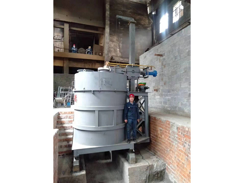
Fig. 2 Crystalline Silicon Preparation Equipment - DC Arc Furnace
3.2 Preparation of High-Purity Silicon, Monocrystalline Silicon, and Polycrystalline Silicon
High-purity silicon for the electronics industry is produced by reducing silicon trichlorohydride or silicon tetrachloride with hydrogen. The process is reducing high-purity silicon trichlorohydride SiHCl3 or SiCl4 with hydrogen on hot silicon rods at 1200 °C.
Ultrapure monocrystalline silicon can be prepared by straight pulling or zone melting methods, etc. Zone melting monocrystalline silicon is prepared by utilizing the float zone melting method, so it is also known as FZ silicon monocrystal. Straight-pulling monocrystalline silicon is prepared using the Chernobyl method, known as CZ monocrystalline silicon. These two types of monocrystalline silicon have different characteristics and different device applications: zone fusion monocrystalline silicon is mainly used in high-power devices, only a very small part of the monocrystalline silicon market, in the international market accounted for about 10% or so, and straight pull monocrystalline silicon is mainly used in microelectronic integrated circuits and solar cells, is the theme of the monocrystalline silicon. Compared with zone fusion monocrystalline silicon, straight pull monocrystalline silicon manufacturing cost is relatively low, high mechanical strength, and easy to prepare large-diameter single crystal, so the solar cell field is mainly used in the application of straight pull monocrystalline silicon, rather than zone fusion monocrystalline silicon.
Czochralski method was invented by Poland's J. Czochralski in 1971, so it is also known as Che's method. 1950 Teal and others will be used for the growth of semiconductor germanium monocrystals, and then use this method of growth of straight pull monocrystalline silicon, based on which, Dash proposed a straight pull monocrystalline silicon growth of “necking “technology, G. Ziegler proposed rapid necking growth of fine neck technology, constituting the modern preparation of large diameter dislocation-free straight pull single crystal silicon basic method. The growth of straight-pull monocrystalline silicon has been the main technology for the preparation of monocrystalline silicon, but also the main preparation method of monocrystalline silicon for solar cells.

Fig. 3 Silicon crystal being grown by the Czochralski method at Raytheon
The straight-pull monocrystalline silicon preparation process generally includes polysilicon loading and melting, seed crystal, necking, shoulder release, isometric, and finishing.
Solar cell polysilicon columnar crystals, crystal growth direction vertically upward, is realized through directional solidification (also known as controlled solidification, constrained solidification) process, that is, in the crystallization process, through the control of the temperature field changes, the formation of uni-directional heat flow (growth direction and the direction of the opposite direction of the heat flow), and the requirements of the liquid-solid interface at the temperature gradient is greater than 0, and transverse to the requirements of the absence of a temperature gradient, to form the formation of directional growth of the columnar crystals. Realization of polysilicon directional solidification growth of the four methods are the Brillman method, heat exchange method, electromagnetic ingot casting method, and casting method. Currently, the most common method used by enterprises is the heat exchange method to produce polysilicon. The heat exchange method for the production of cast polysilicon-specific process flow is generally as follows: loading → heating → chemical material → crystal growth → annealing → cooling.
4 Silicon in the Electronics Industry
4.1 Integrated Circuit (IC)
In integrated circuit (IC) manufacturing, silicon wafers serve as the chip's substrate material and have become a core component of modern electronic devices. Most devices such as computers, smartphones, and tablets rely on these silicon-based ICs internally for computing and data processing. Silicon has excellent semiconductor properties, which makes it an ideal material for transistor fabrication. Transistors are the core components of integrated circuits, allowing them to perform switching and logic operations by controlling the flow of electrical current, which is the basis for the complex computing functions of modern chips.
In addition, the abundance of silicon materials and the sophistication of purification technologies further reduce their production costs. Silicon is abundantly available on Earth and can be easily purified to extremely high purity through the zone melting method, which meets the stringent material requirements for integrated circuit manufacturing. This characteristic is not only suitable for large-scale manufacturing but also provides the chip industry with a sustainable source of low-cost materials, making silicon-based ICs the cornerstone for driving the development of the information age.
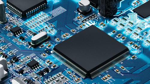
Fig. 4 Integrated Circuit
4.2 Solar Cells
Monocrystalline and polycrystalline silicon, as well as thin films made of silicon, have important applications in solar cells.
Monocrystalline silicon solar cells are made from high-purity monocrystalline silicon, which has the highest photovoltaic conversion efficiency (typically 20% or more) due to its homogeneous cell structure and low lattice defects. Monocrystalline silicon has good light absorption properties and reduces energy loss during photovoltaic conversion. Due to their high efficiency and stability, monocrystalline silicon solar cells are widely used in applications that require high energy density, such as rooftops of homes, commercial buildings, and utility-scale solar power plants. These cells are suitable for long-term installations and situations that require high energy efficiency, and despite their relatively high cost, they can maximize power generation in situations where land use is limited.
Polycrystalline silicon solar cells are cast from blocks of polycrystalline silicon, whose crystalline structure contains a large number of grain boundaries, resulting in slightly lower photovoltaic conversion efficiencies than monocrystalline silicon (typically between 15% and 18%). Polycrystalline silicon materials are less energy-intensive to produce and relatively less expensive. Polycrystalline silicon cells are cost-effective and are therefore commonly used for large solar arrays and for powering utilities and industrial facilities. They are also used in off-grid systems in scenarios such as rural electrification and traffic sign lighting. These cells can provide high power generation while still being cost-effective, making them ideal for widespread installation in ground-mounted solar farms and off-grid areas.
Thin-film silicon solar cells are manufactured by depositing a very thin layer of silicon material on a glass, metal, or plastic substrate. Because of the thin silicon layer, their photovoltaic conversion efficiency is generally low (usually around 10% to 12%), but they are lightweight and flexible. Because of their light weight and flexibility, thin-film silicon solar cells are suitable for building-integrated (BIPV) applications, where they can be mounted directly on building facades, windows, and other surfaces to equip the building structure with power-generating capabilities. In addition, these cells can be used in portable and wearable devices, such as solar backpacks, tents, and other mobile applications to provide power support for small devices.

Fig. 5 Solar Cells
4.3 Microelectromechanical Systems (MEMS) and Sensors
Silicon has a wide range of applications in the field of microelectromechanical systems (MEMS) and sensors, thanks to its excellent mechanical and electrical stability. MEMS devices utilize the properties of silicon to convert mechanical and electrical signals at a micro-scale and are used in a wide range of devices, such as accelerometers, gyroscopes, pressure sensors, etc. These devices play a critical role in automotive airbag systems, smartphone motion sensing, drone balance control, and more. These devices play a crucial role in automotive airbag systems, motion sensing in smartphones, and balance control in drones. In addition, silicon-based sensors can accurately measure environmental parameters such as temperature, humidity, and pressure, making them widely used in automotive, industrial automation, and consumer electronics. Silicon is also used in microfluidic devices, whose microchannel structure enables high-precision control of fluids, and is used in the medical field's “lab-on-a-chip” for detecting tiny substances in liquid samples, which promotes the portable development of disease diagnosis and bioanalysis. These silicon-based MEMS and sensor technologies are driving advances in smart electronics, automation, and biomedical engineering.
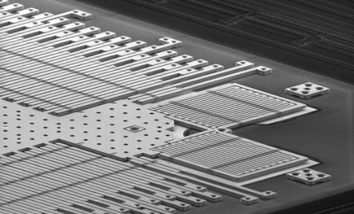
Fig. 6 MEMS
4.4 Power Electronics
Silicon plays an important role in power electronics and is widely used in power semiconductor devices such as MOSFETs and IGBTs. Due to their good conductivity and switching speeds, these devices are particularly suited for high-efficiency energy conversion in applications such as electric vehicles, power converters, and chargers. Silicon power devices also have high power densities and efficiencies, making them widely used in applications requiring efficient transmission, such as data centers, communications base stations, and power supplies. Although silicon's performance in high-temperature and high-voltage environments is relatively limited, its stability and economy in low and medium-power applications are excellent, making it the material of choice for small and medium-power devices. At the same time, to expand the performance and applications of silicon devices, many studies are exploring new silicon-based materials and structures to enhance their performance in high-temperature or extreme environments, fueling the further development of future power electronics technologies.
4.5 Silicon Photovoltaic Applications
Silicon also plays an important role in optoelectronic applications, especially in silicon-based optoelectronics, silicon-based LEDs, and silicon photonics. Silicon photodiodes are widely used in optical communication systems as light detectors and photodiodes in data centers and fiber optic communications to support high-speed, long-distance data transmission. Although silicon is not an ideal light-emitting material, its photoresponsiveness in the infrared band has led to its use in infrared LEDs and chip packaging as well, especially in scenarios where low cost and durability are required. In addition, silicon photonics is emerging as a technology that enables transmission, processing, and computation of optical signals through silicon-based optoelectronic integrated circuits, which can play an important role in 5G, AI computing, and other areas that require high-speed data transmission. These silicon photonics applications drive the development of data communications, information processing, and optical computing, enabling silicon to play a key supporting role in technological advances in the convergence of electronics and optics.
5 Advantages and Limitations of Silicon
5.1 Advantages of Silicon
1. Abundance and sustainability: Silicon is the second most abundant element in the Earth's crust, accounting for more than 27 percent of the crust's mass, and is found mainly in sand and quartz. This means that silicon is extremely abundant, relatively easy to access, and sustainable. The abundance of reserves not only guarantees a stable supply chain for silicon but also makes silicon a reliable option for large-scale industrial production, providing the industry with a guarantee of long-term growth.
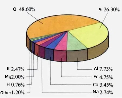
Fig. 7 Elemental content of the Earth's crust
2. Controllable high purity: In the electronics industry, the purity of semiconductor materials is critical. Silicon can be purified by zone melting to achieve extremely high purity levels (over 99.9999%), a level of purity that meets the requirements of high-precision devices such as integrated circuits and transistors. Zone fusion is a highly efficient purification technique that removes impurities by heating specific areas of a silicon rod and slowly moving the fusion zone to achieve an extremely high level of purity within the material within a controlled range. This highly controllable purity allows silicon to excel in many complex electronic applications, especially in microelectronics and integrated circuits.
3. Lower cost: Compared with other semiconductor materials such as gallium arsenide and silicon carbide, silicon is less expensive to extract and process. On the one hand, the natural reserves of silicon are abundant and easy to mine, and the required purification process is relatively mature and suitable for large-scale production. On the other hand, the high stability of silicon makes it less susceptible to loss in manufacturing and processing, which further reduces production costs. As a result, silicon has become the most economical choice in areas such as microprocessors, memory, and solar cells.
5.2 Limitations of Silicon
1. Poor High-Temperature Characteristics: Although silicon behaves stably at room temperature, its conductivity at high temperatures is not ideal. In high-temperature environments, the resistivity of silicon decreases, leading to unstable current flow, which affects device performance. This makes silicon limited in high-power and high-temperature environments, such as aerospace, military electronics, and high-power power converters, where sustained operation at high temperatures is required and silicon's thermal stability is not sufficient to support these applications. These types of requirements often require the selection of materials with better high-temperature performance, such as silicon carbide, to replace silicon.
2. Bandgap limitation: Silicon has a low bandgap (1.1 eV), which, while conducive to high sensitivity in some applications, is undesirable in high-speed and high-frequency devices. The lower bandgap limits the speed at which electrons can switch, making silicon perform less well at high frequencies than other materials with wider bandgaps, such as gallium arsenide, and is therefore limited in high-speed communication applications such as 5G, millimeter-wave devices, and RF power amplifiers. These applications require materials with higher bandgaps to ensure that the devices can support higher frequencies and higher speed data transmission.
6 Conclusion
Silicon’s role in electronics is unparalleled due to its abundance, cost-effectiveness, and unique semiconductor properties. Its high purity and ease of fabrication allow it to excel in areas such as microelectronics, solar energy, and MEMS. However, silicon faces limitations in high-temperature environments and high-frequency applications, where alternative materials like silicon carbide and gallium arsenide are often preferable. Continued advancements in silicon technology aim to address these challenges, ensuring its enduring relevance in the evolution of electronics. Silicon remains indispensable, driving innovation and supporting the ongoing transformation of the digital and renewable energy landscapes.
Stanford Advanced Materials (SAM) is a key provider of high-quality silicon materials, supporting these critical applications with reliable material solutions.
Related reading:
Gallium Arsenide Wafer VS. Silicon Wafer
Graphene Growth and Adherence to Silicon Wafers
The Impact of Silicon Wafer Quality on Semiconductor Performance and Reliability


