Essential Electronic Materials: Part 3 - Germanium
1 Introduction
Germanium (Ge) is a semiconductor material with unique physical and electrical properties, making it a valuable component in various high-tech applications. With an atomic number of 32 and a density of 5.323 g/cm³, germanium has a diamond-like crystal structure that allows it to exhibit excellent electrical conductivity at low temperatures due to its small bandgap of 0.66 eV. This property makes it a superior material for low-temperature electronics and infrared optoelectronics, including fiber-optic communications and infrared detectors. Despite being outshined by silicon (Si) in most semiconductor technologies, germanium remains crucial in high-frequency, high-speed electronics, solar cells, and quantum computing. Its ability to integrate with silicon also presents opportunities for advanced integrated circuit technologies. However, challenges such as lower thermal conductivity, higher costs, and difficulties in large-scale crystal growth limit its widespread application, especially compared to silicon, which dominates the semiconductor industry.
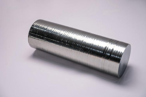
Fig. 1 Germanium Single Crystal
2 Basic Properties of Germanium
Germanium (Germanium) is a chemical element with the atomic number 32 and an atomic weight of 72.64. In the Periodic Table of Elements, it is located in the 4th period and group IVA. In nature, germanium has five stable isotopes: 70Ge, 72Ge, 73Ge, 74Ge, 76Ge. At temperatures above 700°C, germanium reacts with oxygen to form GeO2_2, and above 1,000°C, it reacts with hydrogen. Finely powdered germanium can burn in chlorine or bromine. Germanium is an excellent semiconductor, widely used as a high-frequency current detector and an alternating current rectifier. Additionally, it is used in infrared optical materials, precision instruments, and as a catalyst. Germanium compounds can manufacture fluorescent panels and a variety of high-refractive-index glass. In the periodic table, germanium belongs to the same group as tin and lead, both of which were discovered and utilized by ancient civilizations. However, germanium has not been mined on an industrial scale for a long time. This is not due to the small germanium content in the earth's crust, but because it is one of the most dispersed elements in the earth's crust, germanium-containing ores are rare.
Germanium (Ge) has unique physical properties. Its crystal structure is diamond-shaped, with each germanium atom connected to four neighboring atoms by covalent bonds to form a tetrahedral structure. Germanium has a density of 5.323 g/cm³, a melting point of 937.4°C, a boiling point of 2833°C, and a thermal conductivity of about 60 W/(m-K), which is low compared to metallic materials. As a semiconductor, germanium has a high conductivity at room temperature (about 1.6 × 10³ S/m) and a bandgap width of 0.66 eV, which gives it better conductivity than silicon (Si) at low temperatures but poorer performance at high temperatures. The direct bandgap property of germanium makes it excellent in infrared optoelectronic applications, susceptible to infrared light at 1.55 μm wavelength, and thus widely used in fiber optic communications, infrared detectors, and other fields. Although germanium is chemically stable at room temperature, it may be greatly affected at high temperatures. Its brittleness is high and its hardness is 6.0 Mohs, which limits its application under some high mechanical strength requirements. Although most modern electronic devices are made of silicon, germanium still has important applications in high-speed electronics and infrared technology, especially at low temperatures and high frequencies.
Table 1 Physical Properties of Germanium
Appearance | Finish dark blue, crystalline, silvery-white brittle metal |
Valence | +2, +4 |
First Ionization Energy | 7.899eV |
Solubility | Insoluble In Water |
Atomic Volume | 13.6cm3/mol |
Relative Atomic Mass | 72.64 |
Mohs Hardness | 6 |
The Rate of Propagation of Sound In | 5400m/s |
Density | 5.35g/cm3 |
Melting Point | 937℃ |
Boiling Point | 2830℃ |
Heat And Light Coefficient | dn/dT≈0.0004/K (25~150℃) |
3 Germanium Fabrication Processes
3.1 Czochralski Method
The Czochralski method is a common single-crystal growth technique widely used for the preparation of various types of semiconductor single crystals, including germanium single crystals. The straight pulling method is used to obtain large-sized, high-quality germanium single crystals by pulling liquid crystals of germanium or germanium alloys in the molten state out of a molten pool, gradually cooling them and crystallizing them, and ultimately obtaining large-sized, high-quality germanium single crystals. This method is commonly used in the semiconductor industry, especially in the preparation of germanium materials, as it is capable of producing single crystals with high purity and low defects.
High-purity germanium (Ge) is usually used as the raw material, or germanium alloys (e.g., germanium and silicon alloys) are used as the solution source. High-purity germanium is typically 99.999% pure or higher. The Czochralski method commonly employs an inductive heating furnace or another type of high-temperature furnace to heat germanium. Inside the furnace, molten germanium is contained in a vessel made of highly heat-resistant materials, such as quartz or platinum, to prevent chemical reactions with the germanium. Germanium has a melting point of 937.4°C, so the temperature of the melt needs to be set slightly above this, usually between 1050°C and 1150°C. This ensures that the germanium remains in a liquid state. This ensures that the germanium remains in a liquid state and facilitates the growth of the crystals.
The germanium feedstock is first placed in a furnace and inductively heated to melt it into a liquid state. It is necessary to ensure that the melt remains homogeneous to avoid impurities and bubbles.
The crystal seed is the initial single crystal used to guide the crystal growth. In the Czochralski method, the commonly used material for the crystal seed is pure germanium single-crystal wafers. Germanium single crystal wafers with high quality and perfect lattice are selected as the crystal seed. The crystal orientation of the seed needs to be the same as that of the target single crystal, usually the <100> or <111> crystal plane of germanium. The crystal seed is immersed vertically into the surface of the molten germanium and crystal growth begins at the temperature of the molten pool. Upon contact of the seed with the melt, germanium atoms in the melt gradually attach to the surface of the seed to form a single crystal structure.
On the contact surface between the crystal seed and the molten pool, the crystals begin to grow outward. Slowly and steadily, the seed is pulled vertically out of the melt pool, while controlling the temperature and pulling speed to ensure uniform crystal growth. The pulling speed is usually in the range of 0.5-2 mm/min. Too fast a pulling speed may lead to crystal defects, while too slow a pulling speed may lead to oversized crystals that are difficult to control. The temperature gradient must be precisely controlled to ensure the quality and structure of germanium single crystals. Typically, the temperature decreases as the crystals are pulled from the melt, and the crystal growth rate slows down accordingly. The direction and size of crystal growth can be controlled by controlling the temperature in the upper cooling zone. To avoid germanium oxidation at high temperatures, the growth process is usually carried out in a vacuum or an inert gas (e.g., argon) atmosphere.
Under the guidance of the crystal seed, germanium single crystals will gradually grow to form large single crystals. As the crystal continues to grow, the germanium single crystal gradually increases in diameter and length. The straight drawing method can produce large germanium single crystals ranging from a few millimeters to several inches in diameter. Once the germanium single crystal has grown to the desired size, it will begin to cool slowly. The cooling process requires strict temperature control to avoid temperature differential stresses or thermal cracks within the crystal. Progressive cooling is often employed to gradually move the crystal from a high-temperature region to a room-temperature region, ensuring controlled cooling and reducing the risk of structural defects.
Germanium single crystals prepared by the Czochralski method usually have low defect density, complete crystal structure, and low impurity content. Some lattice defects, such as dislocations, microcracks, etc., may appear during the growth process, which usually requires quality inspection through X-ray diffraction, optical microscopy, or electron microscopy. The electrical properties (e.g., carrier concentration, mobility, etc.) and optical properties (e.g., transmittance, absorption coefficient, etc.) of germanium single crystals are also important indicators for evaluating their quality.
Once the germanium single crystal is cooled and reaches a predetermined size, the crystal can be cut into desired sheets or other shapes. Common processing methods include cutting, polishing, and doping. In some applications, germanium single crystals may need to be doped with certain elements (e.g., phosphorus, boron) to modulate their electrical properties. Doping is usually achieved by diffusion or the addition of a dopant after the crystal growth process.
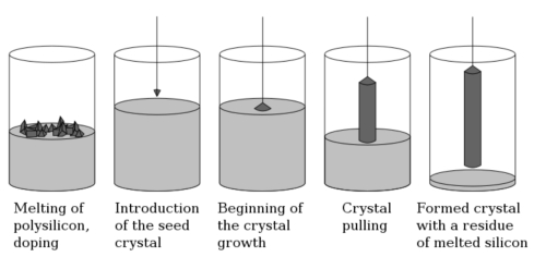
Fig. 2 Principle of Czochralski Method
3.2 Vertical Gradient Freezing Method
The Vertical Gradient Freezing method (VGF method) is a technique commonly used to prepare high-purity single crystals and is particularly suitable for the growth of semiconductor materials such as germanium single crystals. Unlike the Czochralski method, the Vertical Gradient Freezing method realizes the growth of single crystals by controlling the temperature gradient, which has unique advantages in the preparation of high-quality, low-defect semiconductor materials.
The vertical gradient method is a technique that utilizes a temperature gradient to drive crystal growth. The basic principle is to control the transition region of the material from liquid to solid by placing the molten semiconductor material in a region with a large temperature gradient and utilizing this temperature difference to control the crystal growth direction and process. Typically, the melt forms a vertical temperature gradient from top to bottom, resulting in higher temperatures at the top of the melt and lower temperatures at the bottom. The key to the VGF method is that by precisely controlling the temperature gradient of the melt, the melt solidifies gradually from the lower part and can form a single-crystal structure that is free of defects or has low defects.
Carrying out the vertical gradient method for the preparation of high-purity germanium requires the preparation of the melt first. High-purity germanium is placed in a special crucible, which is usually made of high-temperature resistant quartz or platinum. The material contained in the crucible is heated above the melting point and kept in a liquid state. Thereafter a vertically oriented temperature gradient is created in the equipment by controlling the temperature above and below the melt. Typically, the lower part of the melt is kept at a lower temperature (close to the melting point), while the upper part is kept at a higher temperature. With this temperature gradient, the material gradually solidifies from top to bottom. The size and direction of the temperature gradient is critical and determines the rate of crystal growth, the size of the grains, and the quality of the single crystals.
In the cooling region of the melt, the crystal seed is usually placed in the lower temperature zone (i.e., the lower part of the melt). During the gradual decrease in temperature, the melt solidifies and the seed begins to contact the melt and directs the growth of the crystals. As the temperature decreases, the crystals start to grow upwards from the seed until the entire melt in the crucible gradually solidifies into a single crystal structure. In the VGF method, the rate of crystal growth is controlled by adjusting the cooling rate (i.e., temperature gradient). The growth rate is usually slow to ensure that the crystals can grow gradually with low defects. Controlling the crystal growth rate helps to minimize defects and improve the quality of the crystals. In some cases, growing too fast can lead to dislocations or other defects in the crystal.
After the crystal growth is completed, the temperature is gradually reduced to ensure that the whole process is carried out stably. The crystals are gradually solidified from the molten pool into single crystals, and cooling also requires a slow reduction in temperature to avoid stresses and cracks due to sudden temperature changes.
The VGF method has some unique advantages that enable the production of very high-quality single crystals, especially in terms of low defect density and fewer lattice distortions. Due to the more stable temperature gradient during crystal growth, excessive dislocations or other lattice defects in the crystals can be effectively avoided. Since the method has a high control precision during the growth process and can effectively remove some impurities, the VGF method is particularly suitable for the production of high-purity semiconductor materials, especially in optoelectronic devices, and high-frequency devices are more widely used. Compared with the Czochralski method, the VGF method usually adopts a lower crystal growth rate, which helps to obtain a more homogeneous crystal structure and reduces the generation of internal stresses, thus improving the overall performance of single crystals. Moreover, the VGF method does not need to stretch the crystals, which avoids the problems of crystal rupture and uneven growth that may occur during the stretching process and is especially suitable for the preparation of some brittle materials. Through the VGF method, large-size, high-quality single-crystal materials can be prepared more easily, which is very important in some high-end electronics, photovoltaic and solar cells, and other applications.
However, since the VGF method requires a more precise temperature control system, the equipment cost is higher. In particular, the equipment needs to have a high level of technology in terms of temperature gradient control and cooling rate control of the melt. In addition, the VGF method usually has a slower growth rate than the straight drawing method, so the whole growth process takes longer. This may not be as efficient as other methods (e.g., Czochralski's method) in terms of production efficiency, especially when high-volume production is required. Although the VGF method is suitable for the preparation of high-purity materials, it has high requirements for physical properties such as melting point and thermal conductivity of the materials and therefore does not apply to all materials, especially some materials with high melting point or poor thermal conductivity.
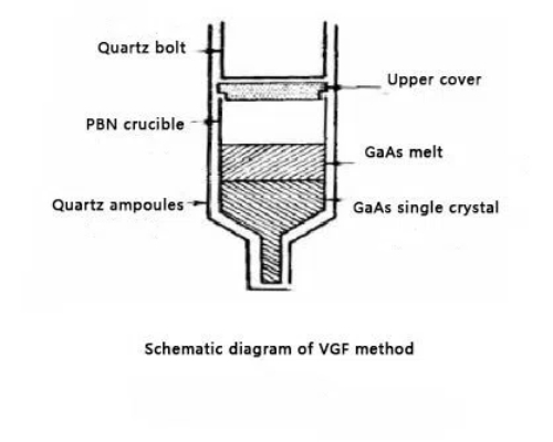
Fig. 3 Schematic Diagram of VGF Method
4 Applications of Germanium
1. High-speed electronics: The high electron mobility of germanium (about twice that of silicon) makes it very promising for use in high-frequency, high-speed electronics. Especially in microelectronic devices that require high-speed switching, germanium helps increase operating speed and efficiency. Because germanium has a lower energy bandwidth and higher carrier mobility, it can provide better performance in high-frequency applications. This has led to the use of germanium in applications such as wireless communications, radio frequency (RF) amplifiers, and UHF amplifiers.
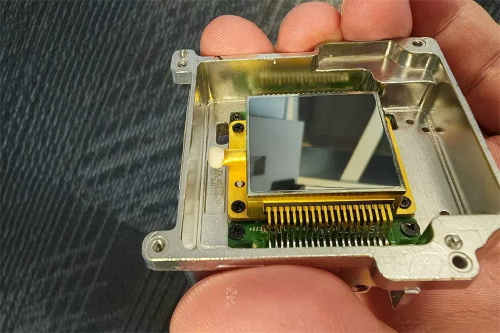
Fig. 4 Germanium Chip
2. Infrared Optical Materials: Germanium has excellent transmittance in the mid-infrared band (2-12 μm), making it an ideal material for infrared detectors and imaging systems. For example, germanium is widely used in devices such as infrared sensors and infrared cameras, especially in military, security, and climate monitoring. Germanium's small band gap (about 0.66 eV) allows it to respond effectively to infrared radiation at room temperature. Compared to silicon, germanium has a more sensitive response in the long-wave infrared region, making it more widely used in applications such as infrared detectors and infrared imaging systems.
3. Optical fiber communications: Germanium is often doped into optical fibers, especially germanium-doped SiO₂ (Ge-doped SiO₂) fibers, to improve the performance of optical fibers. Germanium-doped optical fibers have a higher refractive index and can transmit optical signals more efficiently. Therefore, germanium materials are widely used in fiber optic communications as a core material and gain medium. In photoelectric conversion devices, germanium is also used as an efficient photoelectric conversion material. Due to its excellent infrared responsivity, germanium is used in solar cells and other photodetectors.
4. Integrated circuits (ICs) and transistors: With advances in silicon technology, alloys of germanium and silicon (e.g., SiGe alloys) are widely used in integrated circuits. SiGe technology provides higher electron mobility and lower power consumption for high-speed, high-frequency applications, such as microprocessors and radio-frequency integrated circuits. In high-performance integrated circuits (e.g., high-speed transistors), especially in quantum effect and nanotechnology applications, germanium is used as a high-mobility material to enhance device performance. By integrating germanium onto silicon substrates, the performance of transistors can be dramatically enhanced, especially at the micrometer and even nanometer scales.
5. Semiconductor lasers (LDs): Germanium materials are used in the fabrication of semiconductor lasers, especially in near-infrared (NIR) laser applications. Germanium has a small bandgap and is capable of producing optoelectronic properties different from those of silicon materials, making it suitable for low-energy consumption and high-efficiency semiconductor lasers. The germanium-silicon structure is one of the hotspots of current research, and the combination of germanium and silicon can help develop silicon-based lasers for optical communications, optical interconnects, and other applications.
6. Solar cells (photovoltaic technology): germanium is suitable for use as a substrate in photovoltaic materials due to its low band gap (0.66 eV), and is usually combined with other materials (e.g. silicon) to form multi-junction solar cells. The application of germanium in multi-junction solar cells can effectively absorb a wider range of spectra and enhance the conversion efficiency of solar cells, which has great potential, especially in space satellites and high-efficiency solar applications. Germanium is widely used in space solar cells and high-efficiency photovoltaic devices in aerospace due to its stable photoelectric conversion performance.

Fig. 5 Solar Panel
7. Charge-coupled devices (CCDs): Germanium materials are also widely used in charge-coupled device (CCD) sensors, which are used in areas such as image sensing, videography, and microscopy technology. Germanium's high electron mobility and excellent electrical properties enable it to provide better detection capabilities under low-light conditions.
8. Laser radar (LiDAR): Germanium materials also have important applications in laser radar (LiDAR) systems, particularly in high-precision ranging, environmental scanning, and autonomous driving technology. The high responsiveness of germanium makes it superior in the short-wave infrared spectral range, making it an ideal material for efficient laser detection.
9. Quantum computing and quantum technology: Germanium materials have potential in quantum computing, especially when building quantum bits. Because of its compatibility with silicon, scientists are looking at using germanium to develop silicon-based quantum computing systems to develop more powerful quantum computers. Germanium is also being explored for use in quantum sensors and quantum communications, where more efficient quantum sensing devices can be constructed by utilizing its good electrical properties and low defect characteristics.
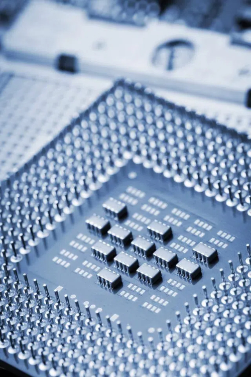
Fig. 6 Germanium for Quantum Computers
5 Advantages and Limitations of Germanium
5.1 Advantages of Germanium
1. High Electron Mobility: Electron mobility is an important measure of the ability of electrons to move through a semiconductor material, and germanium has a higher electron mobility than silicon (Si), about twice that of Si (about 3900 cm²/V-s). This means that germanium outperforms silicon in high-speed electronics such as high-speed transistors, providing higher switching speeds and lower power consumption.
The high mobility gives germanium an advantage in high frequency (RF) and high-speed communications, enabling more efficient signal transmission.
2. Low Bandgap Characteristics (0.66 eV): Germanium has a small bandgap (0.66 eV), which allows it to exhibit high conductivity at low temperatures or low energy. This characteristic makes germanium very suitable for infrared optoelectronic devices (e.g., infrared detectors, fiber optic communications, etc.).
The low bandgap also gives germanium an advantage in certain high-efficiency photovoltaic conversion devices (e.g., solar cells), especially in the bottom layer of multi-junction solar cells, where it can effectively absorb long-wavelength spectra.
3. High transmittance (infrared spectrum): Germanium has a very high light transmittance (2-12 μm) in the mid-infrared region, making it an ideal material for infrared imaging, infrared detectors, and other fields. In these applications, germanium can increase the sensitivity and accuracy of devices.
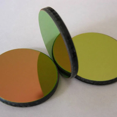
Fig. 7 Infrared Germanium Glass
This makes germanium play an important role in infrared sensors for military detection, climate monitoring, security, and other fields.
4. Good compatibility with silicon: Germanium has a good crystal structure that matches silicon and can form alloys (e.g., SiGe alloys), thus giving full play to the advantages of silicon and germanium. For example, SiGe alloys used in integrated circuits (ICs) can significantly improve the performance of high-speed ICs.
The compatibility between germanium and silicon makes it possible to integrate germanium in silicon-based electronics, especially in high-frequency, high-speed devices.
5. Suitable for high-efficiency solar cells: Due to its small bandgap, germanium can effectively absorb the long wavelength portion of the spectrum, especially as a lower layer material in multi-junction solar cells, enhancing the photoelectric conversion efficiency of solar cells. The high efficiency of germanium makes it widely used in space solar cells in space applications.
6. Potential in quantum computing: The low-defect properties of germanium materials make them potentially useful in quantum computing, especially in the construction of quantum bits (qubits). The compatibility between germanium and silicon makes it an ideal building material for integrated quantum bits in quantum computing, especially important in silicon quantum computing research.
5.2 Limitations of Germanium
1. Lower thermal conductivity: The thermal conductivity of germanium (about 60 W/m-K) is much lower than that of silicon (about 150 W/m-K). This means that in high-power density semiconductor devices, germanium has a poor ability to dissipate heat, which can easily lead to heat buildup, thus affecting the stability and long-term reliability of the device.
The degradation of performance at high temperatures and the heat dissipation problem are the main limiting factors for germanium materials in high-power applications.
2. Higher price: The raw material cost and production cost of germanium are higher, especially since the preparation process of high-purity germanium is complicated and requires a sophisticated crystal growth process. As a result, germanium is more expensive to manufacture than silicon, which makes it difficult to adopt widely in certain cost-sensitive applications.
Despite its advantages in high-end applications, germanium's high cost limits the spread of large-scale commercialized applications, especially in some consumer electronics fields that require low cost.
3. Growth technology and crystal quality issues: germanium single crystal growth is more difficult, especially in the preparation of high-quality, large-size germanium single crystals, the need for high-precision growth control technology, such as straight pulling method (Czochralski method), Vertical Gradient Factor (VGF method) and so on. The production and application of germanium crystals are somewhat constrained due to the complexity and cost of these techniques.
Germanium may have dislocations, defects, or impurities in its crystal structure, which affects its application in high-performance electronic devices.
4. Limited industrial production scale: Although germanium performs well in high-end applications, the current production scale and equipment investment in germanium are still not comparable to that of silicon. The supply chain for germanium materials is not as mature and extensive as that for silicon, which limits its popularity in some large-scale applications, especially in consumer electronics and low-cost devices.
6 Conclusion
Germanium offers significant advantages in fields where high-speed electronics, infrared sensitivity, and optoelectronic capabilities are essential. Its superior electron mobility, low bandgap, and compatibility with silicon make it ideal for high-performance applications in communication systems, infrared imaging, and energy-efficient solar cells. However, germanium’s use is constrained by several limitations, including its lower thermal conductivity, higher production costs, and challenges in large-scale manufacturing. Despite these hurdles, germanium remains a critical material in advanced electronics, particularly in niche applications requiring high precision and performance. Continued innovation in germanium fabrication techniques and its integration with silicon-based technologies could expand its role in emerging fields like quantum computing and next-generation optoelectronics.
Stanford Advanced Materials (SAM) is a key provider of high-quality germanium materials, supporting these critical applications with reliable material solutions.
Related Reading

