Innovative Coating Techniques for Laser Crystal Wafers
1 Introduction
In the fast-evolving fields of photonics, telecommunications, and advanced manufacturing, laser crystal wafers are foundational components. Their efficiency and longevity depend heavily on one critical factor: surface coatings. As demand grows for higher-power lasers, ultra-precise optics, and devices resistant to extreme environments, traditional coating methods are being outpaced. This article explores cutting-edge coating technologies revolutionizing laser crystal wafer performance—and why they matter for your next project.
2 Why Coatings Matter for Laser Crystal Wafers
Laser crystal wafers (e.g., Nd: YAG, Ti: Sapphire ) generate and amplify light, but their surfaces are vulnerable to damage from high-energy photons, thermal stress, and environmental contaminants. Advanced coatings serve dual purposes:
1. Optical Enhancement: Anti-reflective (AR) coatings minimize light loss at interfaces.
2. Protection: Hard coatings shield against scratches, moisture, and thermal degradation.
3. Functionality: Dichroic or frequency-selective coatings enable wavelength-specific applications.
Innovations in coating techniques now address challenges like sub-nanometer precision, adhesion durability, and scalability—critical for industries from quantum computing to medical lasers.
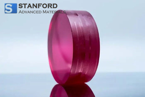
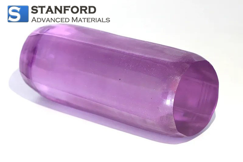
Fig. 1 Ti: Sapphire (Titanium-doped Sapphire Crystal)
3 Breakthrough Coating Technologies to Watch
3.1 Atomic Layer Deposition (ALD)
Atomic Layer Deposition is a method that allows substances to be plated onto the surface of a substrate layer by layer in the form of a single atomic film. Atomic layer deposition is similar to ordinary chemical deposition (chemical vapor deposition). However, in atomic layer deposition, the chemical reaction of the new atomic film is directly related to the previous one, in such a way that only one layer of atoms is deposited per reaction. The primary reactants in atomic layer deposition are two chemicals, often referred to as precursors. The precursors react with the surface of the material in a continuous, self-limiting manner. Thin films are deposited slowly by reacting separately with different precursors. Atomic layer deposition is a key semiconductor device assembly method and can also be a part of some nanomaterial synthesis methods.
Atomic layer deposition is a method (technique) of forming a deposition film by pulsating alternating pulses of gas-phase precursors into a reactor and chemisorbing and reacting on a deposition substrate. When the precursors reach the surface of the deposition substrate, they chemisorb and react on the surface. The atomic layer deposition reactor needs to be cleaned with an inert gas between precursor pulses. It can be seen that the ability of the precursor substances of the deposition reaction to chemisorb on the surface of the deposited material is the key to the realization of atomic layer deposition. The surface adsorption characteristics of gas-phase substances on the substrate material can be seen, any gas-phase substances on the surface of the material can be physically adsorbed, but to be chemically adsorbed on the surface of the material must have a certain activation energy, and therefore whether to achieve atomic layer deposition, the selection of a suitable reaction precursor material is very important.
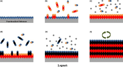
Fig. 2 Process of Atomic Layer Deposition (ALD)
The surface reaction of atomic layer deposition is self-limiting, and in fact, this self-limiting feature is the basis of atomic layer deposition technology. Repetition of this self-limiting reaction results in the formation of the desired film.
Atomic Layer Deposition (ALD) revolutionizes laser crystal wafer coatings by delivering unmatched uniformity and material versatility. Through its precise, layer-by-layer gas-phase reactions, ALD creates ultra-thin, conformal films that evenly coat even the most intricate geometries and microstructured surfaces—eliminating weak spots common in traditional methods. This uniformity is critical for applications like quantum cascade lasers and UV/IR optics, where angstrom-level thickness control ensures peak performance. Additionally, ALD’s flexibility in material selection enables tailored solutions, from protective aluminum oxide (Al2O3) layers to anti-reflective silicon dioxide (SiO2) coatings, alongside hybrid stacks combining nitrides like titanium nitride (TiN) with oxides. Such adaptability makes ALD indispensable for advancing photonic devices requiring both precision and multifunctionality.
Atomic Layer Deposition (ALD) excels in applications demanding angstrom-level precision, making it indispensable for cutting-edge technologies like quantum cascade lasers and UV/IR optical systems, where even nanometer-scale deviations can compromise performance. This technique’s ability to achieve atomic-scale uniformity ensures flawless coatings for wavelength-specific optics and high-energy laser components. These capabilities position ALD as the go-to solution for high-precision R&D laboratories and manufacturers specializing in miniaturized photonic devices, such as integrated optical circuits or micro-lasers, where rigorous thickness control and material consistency are non-negotiable. By enabling repeatable, defect-free coatings on complex microstructures, ALD empowers innovators to push the boundaries of photonics miniaturization and efficiency.
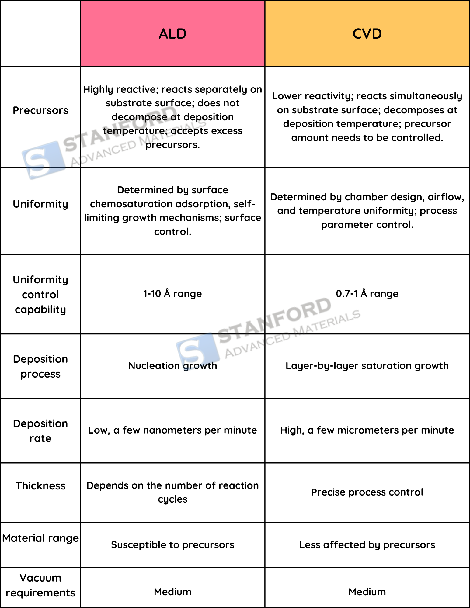
Table 1: Comparison of ALD technology with CVD technology
3.2 Ion Beam Sputtering (IBS)
Ion beam deposition technology is a revolutionary surface processing and modification methods, its core equipment through the ionization source (such as argon ions or nitrogen ions) to generate high-energy ion beams, through the focusing and directional system to accurately regulate the energy density and incidence angle, and ultimately bombardment of the surface of the material to achieve the atomic level of deposition or modification. With high energy density and precise controllability, this technology shows significant advantages: fast deposition speed, excellent uniformity of the film layer, accurate control of the composition and thickness, and even adaptability to the surface treatment of complex three-dimensional structures. In semiconductor manufacturing, it is used to prepare high-purity conductive films; in the optical field, it can be coated with ultra-hard transmittance enhancement film; in aerospace devices, it is used to enhance the material's resistance to high temperatures and corrosion resistance. With the miniaturization of microelectronic devices and the explosion of nanomaterials demand, ion beam deposition technology is becoming a core tool for functional materials research and development and high-end manufacturing, with unlimited potential in the future in the field of flexible electronics, quantum devices, and other cutting-edge technologies.
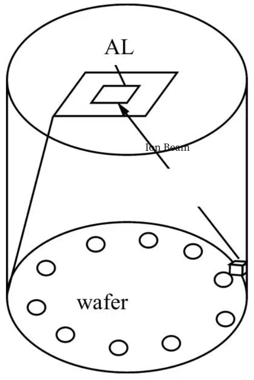
Fig. 3 Ion Beam Sputtering
3.3 Plasma-Enhanced Chemical Vapor Deposition (PECVD)
Plasma-Enhanced Chemical Vapor Deposition (PECVD) is a sophisticated thin-film fabrication method that leverages plasma energy to drive chemical reactions, converting gaseous precursors into solid-state coatings on substrates. Unlike traditional CVD processes, PECVD operates by first ionizing precursor gases (e.g., silane, ammonia) into a reactive plasma state, typically generated through radio frequency (RF) or direct current (DC) electrical discharges between electrodes within a gas-filled chamber. This plasma energizes gas molecules, breaking chemical bonds and initiating reactions that deposit ultra-thin, highly uniform films—from silicon nitride dielectrics to diamond-like carbon coatings. Key advantages include low-temperature processing (ideal for heat-sensitive materials like polymers) and tunable film properties (e.g., stress, density, stoichiometry), making PECVD indispensable for semiconductor interconnects, optical coatings, and flexible electronics manufacturing. By balancing precision with scalability, it bridges lab-scale innovation and industrial production demands.
Plasma-Enhanced Chemical Vapor Deposition (PECVD) stands out for its ability to integrate multi-functional properties—such as optical transparency, hydrophobicity, and electrical conductivity—into a single film layer during deposition, eliminating the need for sequential processing. This versatility is paired with low thermal budget, enabling safe deposition on delicate substrates like polymer-bonded laser crystals or flexible electronics without thermal degradation. Furthermore, PECVD’s compatibility with batch processing streamlines large-scale production, slashing costs while maintaining uniformity across complex geometries. These attributes make it a game-changer for medical laser components (e.g., biocompatible coatings) and consumer electronics (e.g., scratch-resistant, anti-reflective smartphone screens), where multifunctional coatings and rapid scalability are critical to meeting market demands.
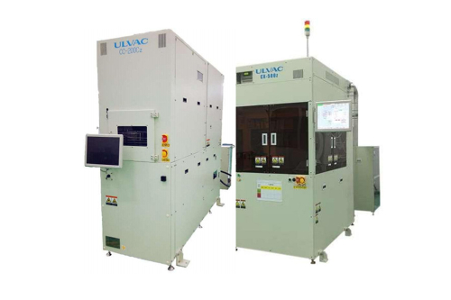
Fig. 4 Plasma-Enhanced Chemical Vapor Deposition (PECVD) Facilities
3.4 Hybrid Coating Systems
Combining techniques like ALD with magnetron sputtering or sol-gel processes allows engineers to "stack" coatings with tailored properties. For example, A hard SiO2 outer layer (via IBS) + AR inner layer (via ALD) = Scratch-resistant, high-transmission optics. Graded-index coatings reduce interfacial stress for high-power laser diodes.
4 Key Considerations When Selecting a Coating Technology
4.1 Performance Needs: Performance Needs
Wavelength Range: Coatings must be designed to precisely match the wavelength at which the laser system operates. For example, ultraviolet (UV) lasers require wide bandgap materials (e.g., Al2O3) that are resistant to high-energy photons, whereas infrared (IR) systems may rely on multilayered dielectric coatings to achieve low-loss reflectivity.
Power Density: High-power lasers, such as fiber lasers for industrial cutting, require coatings with very low absorption and high thermal conductivity to avoid thermal lensing effects or coating ablation. For example, Ta2O5/SiO2 high reflective films prepared by ion beam sputtering (IBS) can withstand power densities of >10 MW/cm².
Environmental Exposure: Laser components used in outdoor or industrial environments need to resist humidity, salt spray, or chemical corrosion. For example, an Al2O3 encapsulation layer deposited by ALD can significantly improve device life in humid environments.
4.2 Substrate Compatibility: Substrate Compatibility
Thermal Expansion Coefficients: Differences in thermal expansion between the coating and the substrate can lead to interface cracking under temperature cycling. For example, a sapphire (Al2O3) substrate has a similar coefficient of thermal expansion to a SiO2 coating (~8 ppm/K), which is a better fit than a silicon substrate (~3 ppm/K).
Chemical Stability: Precursor gases or plasma need to avoid reacting with the substrate during deposition. For example, when depositing silicon nitride (SiNₓ) by PECVD, the flow of ammonia (NH3) needs to be controlled to prevent the etching of the organic polymer substrate.
4.3 Cost vs. Precision: Trade-off between Cost and Precision
Atomic Layer Deposition (ALD): Although ALD can achieve atomic level thickness control (±0.1 nm), the deposition rate is low (~1 nm/min), and the equipment and process costs are high, which makes it suitable for low-volume, high-value-added products (e.g., quantum dot lasers).
Magnetron Sputtering (Magnetron Sputtering): lower cost and suitable for large-area coating (e.g., photovoltaic panels), but the uniformity of the film layer (±5%) and interface roughness is slightly inferior to ALD, commonly used in consumer electronics optical components.
Balancing strategy: Hybrid processes (e.g., ALD+sputtering) can balance critical interface accuracy with overall cost, such as coating a 5 nm adhesion layer with ALD and then sputtering a functional layer.
4.4 Regulatory Compliance
RoHS (Restriction of Hazardous Substances Directive): Restriction of cadmium (Cd), lead (Pb) and other 6 types of substances, affecting the choice of coating materials. For example, traditional cadmium-containing IR transmittance enhancement films need to be replaced with ZrO2/Y2O3 systems.
REACH (Registration and Evaluation of Chemicals): Toxicological evaluation is required for chemical substances with an annual sales volume >1 ton in the EU market. For example, ALD precursor trimethylaluminum (TMA) requires an exposure scenario analysis report.
Biocompatibility (ISO 10993): Medical laser devices (e.g., endoscope coatings) are required to pass cytotoxicity tests, with preference given to biologically inert materials (e.g., diamond-like carbon films).
Scenarios | Prioritized Technologies | Key Considerations |
High-power laser weapon mirrors | IBS | Low optical loss, high damage thresholds |
Flexible biosensor electrodes | PECVD | Low-temperature process, conductive/biocompatible bifunctionality |
5G RF filter wafers | ALD | Sub-nanometer thickness uniformity, RoHS-compliant precursors |
5 Conclusion
From the nanoscale precision of atomic layer deposition (ALD) to the multifunctional integration of plasma chemical vapor deposition (PECVD), laser crystal wafer coating technologies are reshaping the field of optoelectronics and high-end manufacturing with disruptive innovations. These technologies not only address the thermal management bottlenecks of high-power lasers and the need for surface functionalization of complex optics but also open the path from lab to mass production through scalable process designs (e.g., batch PECVD, hybrid ALD-sputtering systems). The choice of coating solution anchors wavelength compatibility, substrate thermal/chemical stability, and compliance (e.g., RoHS lead-free requirements) while weighing precision and cost - for example, treating critical interfaces with ALD, followed by magnetron sputtering for large surface deposition. With the explosion of emerging applications such as quantum communications and biomedical lasers, coating technology will continue to evolve toward ultra-low defect rates and intelligent process control.
Stanford Advanced Materials (SAM) is a leading supplier of high-quality laser crystals, delivering reliable solutions to meet the diverse needs of various industries.
Related Reading