Essential Electronic Materials: Part 4 - Gallium Compounds
1 Introduction
Gallium-based compounds, including gallium oxide (Ga2O3), gallium arsenide (GaAs), and gallium nitride (GaN), have garnered significant attention in the field of electronic and semiconductor materials due to their exceptional physical and chemical properties. These materials exhibit a diverse range of electrical, optical, and thermal characteristics, making them indispensable for advanced technologies.
Gallium oxide (Ga2O3), with its ultra-wide bandgap and high breakdown electric field, is emerging as a promising material for high-power electronics, ultraviolet photodetectors, and other optoelectronic applications. Meanwhile, gallium arsenide (GaAs), a direct bandgap semiconductor with superior electron mobility and high-frequency performance, has long been a cornerstone in optoelectronic devices such as lasers, LEDs, and photovoltaic cells. Gallium nitride (GaN), known for its wide bandgap, high thermal conductivity, and excellent efficiency, has revolutionized power electronics and high-frequency communication systems.
The synthesis techniques for these materials—ranging from chemical vapor deposition and molecular beam epitaxy to innovative hybrid processes—play a critical role in achieving the desired crystal quality and performance. As gallium compounds continue to drive advancements in power, optoelectronics, and sensing technologies, understanding their structure, properties, and applications has become vital for researchers and industry professionals alike.
This article provides a comprehensive overview of the structural characteristics, physical properties, fabrication methods, and applications of Ga2O3, GaAs, and GaN, highlighting their current advancements and prospects in the rapidly evolving semiconductor landscape.
2 Gallium Oxide (Ga2O3)
Gallium oxide, with the chemical formula Ga2O3, is an inorganic compound with the chemical formula Ga2O3. It is a wide-band semiconductor with Eg=4.9eV, whose conductivity and luminescence properties have long attracted attention. Ga2O3 is a transparent oxide semiconductor material with broad application prospects in optoelectronic devices. It can be used as an insulating layer in Ga-based semiconductor materials, as a UV filter, and as an O2 chemical detector.
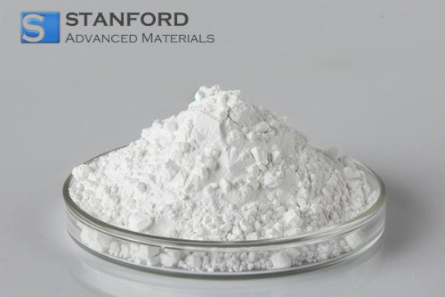
Fig. 1 Gallium Oxide Powder
2.1 Crystal Structure of Gallium Oxide
The five crystal structures of gallium oxide are β-Ga2O3, α-Ga2O3, γ-Ga2O3, δ-Ga2O3 and ε-Ga2O3.
β-Ga2O3, also known as monoclinic gallium oxide, has a monoclinic crystal structure with the space group P21 (a=12.203, b=5.671, c=6.524, and β=105.76). β-Ga2O3 consists of gallium oxide units, which have the characteristics of high electron mobility, wide direct energy gap, and good thermal stability. Currently, β-Ga2O3 is mainly used in the fields of high-power semiconductor devices and deep-ultraviolet optoelectronic devices.
α-Ga2O3, also known as tetragonal crystal system gallium oxide, has a crystal structure of a tetragonal crystal system with space group C4V (a=12.22, c=5.86). α-Ga2O3 is an excellent optical material with high light transmittance and good corrosion resistance. It has a wide range of applications in fields such as optoelectronics and optoelectronic communications.
γ-Ga2O3, also known as cubic crystal system gallium oxide, has a cubic crystal system crystal structure with space group Ia3 (a=13.54). γ-Ga2O3 has high optical transmittance, low defect density, and high magnetic permeability, making it a potential material for use in magneto-optical and UV detector devices.
δ-Ga2O3, also known as orthorhombic crystal system gallium oxide, has an orthorhombic crystal structure with the space group Pnma (a=7.794, b=5.580, c=5.395). δ-Ga2O3 is a material with a high bandgap, excellent photovoltaic properties, and good physicochemical stability, and it has a wide range of applications.
ε-Ga2O3, also known as gallium oxide with a tripartite crystal system, has a crystal structure of a tripartite crystal system with space group R3c (a=12.170, c=24.812). ε-Ga2O3 is a material with high carrier mobility and high thermal stability, and it has good UV response properties. At present, ε-Ga2O3 is mainly used in UV detectors and power electronics fields.
Table 1 Comparison of Different Structures of Ga2O3
| β-Ga2O3 | α-Ga2O3 | γ-Ga2O3 | δ-Ga2O3 | ε-Ga2O3 |
Crystal Structure | Monoclinic Crystal System | Tetragonal Crystal System | Cubic Crystal System | Orthogonal Crystal System | Tripartite Crystal System |
Space Group | P21 | C4V | Ia3 | Pnma | R3c |
Cell Parameters | a=12.203 b=5.671 c=6.524 β=105.76 | a=12.22 c=5.86 | a=13.54 | a=7.794 b=5.580 c=5.395 | a=7.794 b=5.580 c=5.395 |
Properties | High electron mobility | High light transmittance | High optical transmittance | High bandgap | High carrier mobility |
Wide direct energy gap | Good corrosion resistance | Low defect density | Excellent optoelectronic properties | High thermal stability of the material | |
Good thermal stability | - | High magnetic permeability | Good physicochemical stability | Good UV response characteristics | |
Applications | High-power semiconductor devices and deep-ultraviolet optoelectronic devices | Optoelectronics and optoelectronic communications | Potential use in magneto-optical devices and UV detector devices | - | Ultraviolet detectors, power electronics |
2.2 Physical and Chemical Properties of Gallium Oxide
Ga2O3 can react with fluorine gas to produce GaF3, and Ga2O3 dissolved in 50% HF gives the product GaF3-3H2O.Ga2O3 is soluble in slightly hot dilute nitric acid, dilute hydrochloric acid, and dilute sulfuric acid. After burning Ga2O3 is not soluble in these acids or even in concentrated nitric acid, nor aqueous solutions of strong bases, and it can only be made soluble by melting NaOH, KOH, or KHSO4 and K2S2O7 together. Gallium chloride is produced by melting with twice the excess NH4Cl at 250°C. At red heat, Ga2O3 reacts with quartz to form a vitreous body, but no new compounds are formed on cooling. It also reacts with glazed porcelain crucibles at red heat.
Under heated conditions, Ga2O3 can react with many metal oxides. The crystal structure of the gallate M(I)GaO2 obtained by reaction with alkali metal oxides (above 400°C) has been determined, and like Al2O3 and Ln2O3, it reacts with MgO, ZnO, CoO, NiO, and CuO to form the spinel-type M(II)Ga2O4. The product of the reaction with the trivalent metal oxides, M(III)GaO3, usually has chalcocite- or garnet-type structures (e.g., the lanthanide gallate LnGaO3). More complex ternary oxides are also available. Mixed oxides of gallium have been studied for use in lasers, phosphorescence, and luminescent materials. It is believed that the luminescent properties of gallium salts are attributed to oxygen vacancies. Because FeGaO3 has intriguing electromagnetic properties (i.e., piezoelectricity and ferromagnetism), its synthesis, stability, and crystal structure have been studied extensively.
As a semiconductor material, gallium oxide has an ultra-broad forbidden band, with a breakdown electric field strength much higher than that of other broad-band semiconductor materials. It has lower on-resistance at the same voltage level, which reduces energy loss. Although the thermal conductivity of gallium oxide itself is low, the heat dissipation problem can be solved using encapsulation and other means, which contributes to the stable operation of the device at high power density. Gallium oxide devices can also be operated at higher temperatures and are adapted to harsh environments.
2.3 Preparation of Gallium Oxide
1. Direct reduction method: This method gets gallium nitride by reacting nitrogen with gallium metal, and then oxidized to gallium oxide in oxygen. This method can get relatively high-purity gallium oxide, but the process is complicated, needs high temperature and high-pressure environment, and the production cost is high.
2. Chemical vapor deposition method: This method prepares high-purity gallium oxide by transporting a gas mixture into a reaction chamber, where a chemical reaction occurs at a high temperature. Commonly used reaction gases include gallium trichloride (GaCl3).
3. Acid method: This method consists of the following steps:
- Oxidation: add liquid raw material to the reactor, add aqua regia dropwise, and stir, control the temperature at 80-85℃, reaction time of 8±1 hours.
- Neutralization: The generated Ga(NO3)3 and GaCl3 solution is fed into the reaction drum, ammonia is added and stirred to neutralize to pH 7-7.5, and the temperature of the water bath is controlled at 60-70℃.
- Filtration: The solution after the neutralization reaction was filtered through a filter cloth to obtain gallium hydroxide precipitate.
- Washing: The gallium hydroxide precipitate is washed 5-6 times with high-purity water and then filtered.
- Drying: After washing, the gallium hydroxide is put into the drying oven to dry the water, the drying temperature is 150℃, and the drying time is 20±2 hours.
- Roasting: After drying, the gallium hydroxide is put into the roasting furnace to roast and dehydrate, the roasting temperature is 600-700℃, and the roasting time is 3±0.5 hours.
- Grinding: After roasting, the gallium oxide is ground by a grinder to reach the required mesh.
- Packing: Vacuum packing the products into the warehouse
2.4 Applications of Gallium Oxide
1. Power Electronics
Gallium oxide has a breakdown electric field strength of up to 8MV/cm, much higher than other wide-band semiconductor materials, which gives it a significant advantage in high-voltage, high-frequency, and high-power application scenarios. It also has lower on-resistance at the same voltage level, which reduces energy loss and improves energy conversion efficiency. Although gallium oxide itself has a low thermal conductivity, the heat dissipation problem can be solved through encapsulation and other means, which contributes to the stable operation of the device at high power densities. At the same time, gallium oxide devices can work at higher temperatures and adapt to harsh environments. Therefore, gallium oxide has a wide range of application prospects in the field of power electronic devices, such as motor drive systems for electric vehicles, and high-voltage DC transmission systems for smart grids.
2. Optoelectronic Devices
Ultraviolet detector: Gallium oxide has great potential for application in the field of optoelectronics, it can be used to manufacture high-performance ultraviolet detectors with high sensitivity and fast response. These detectors play an important role in environmental monitoring, biomedical, and other fields, such as the detection of ozone concentration in the atmosphere, and the organic content of water.
Deep UV light-emitting diode (LED): The special energy band structure of gallium oxide material enables it to emit deep ultraviolet light with shorter wavelength and higher energy, which has a more significant sterilization effect. Therefore, the deep ultraviolet LED has a wide range of applications in sterilization, and semiconductor manufacturing processes, such as photolithography.
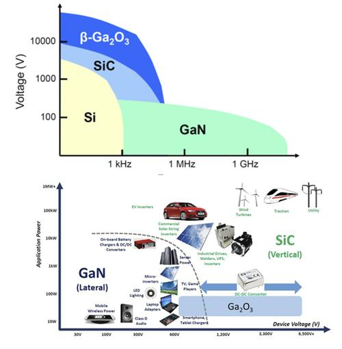
Fig. 2 Comparison of Applications of SiC, GaN and Ga2O3
3. The Sensor
Gallium oxide semiconductor material's special chemical and electrical properties give it a wide range of applications in the field of sensors. It can be used to make humidity sensors, temperature sensors, gas sensors, pressure sensors, and other sensors to meet the needs of different fields.
4. Other Applications
In addition to the above fields, gallium oxide semiconductor material also has applications in other fields. For example, it can be used to make flexible display devices, battery materials, and so on. In addition, with the continuous progress of technology and cost reduction, gallium oxide is also gradually expanding its application in the field of radio frequency, such as radar systems, satellite communications, and wireless base stations.
3 Gallium Arsenide(GaAs)
Gallium arsenide is an inorganic compound with the chemical formula GaAs, a black-gray solid with a melting point of 1,238°C. It can be found in air below 600°C and is not attacked by non-oxidizing acids. It can be stabilized in air below 600°C and is not eroded by non-oxidizing acids. Gallium arsenide is an important semiconductor material. Belongs to the Ⅲ-V compound semiconductor. Is a sphalerite-type lattice structure, lattice constant 5.65 × 10⁻¹⁰m, forbidden band width 1.4 eV.
3.1 Crystal Structure of Gallium Arsenide
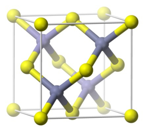
The crystal structure of Gallium Arsenide belongs to the cubic crystal system, face-centered cubic (FCC) structure, Ga atoms are located at the apex of the face-centered cubic lattice, As atoms are located in the face-centered positions of the neighboring Ga atoms, and Ga atoms and As atoms are interconnected with each other by covalent bonding, which makes Gallium Arsenide have electronic conduction properties. The lattice constant of GaAs crystal is a=5.6535Å.
Fig. 3 Crystal Structure of Gallium Arsenide
3.2 Physical and Chemical Properties of Gallium Arsenide
GaAs has some better electronic properties than Si, allowing GaAs to be used above 250 GHz. If the equivalent GaAs and Si components are both operated at high frequencies, GaAs produces less noise. Also, because GaAs has a higher collapse voltage, GaAs is better suited for high-power operation than the same Si component. Because of these characteristics, GaAs circuits can be used in cell phones, satellite communications, microwave point-to-point links, radar systems, etc. GaAs has been used to make Gann diodes, microwave diodes, and Geng diodes to emit microwaves.
Table 2 Physical Properties of Gallium Arsenide
Density | 5.31g/cm3 |
Melting Point | 1238℃ |
Refraction Index | 3.57 |
Relative Permittivity | 13.18 |
Electron Affinity Energy | 4.07eV |
Lattice Energy | 5.65×10⁻¹⁰m |
Band Gap | 1.424e(300K) |
Electron Mobility | 8500cm2/(V·s)(300K) |
Appearance | Black-Grey Solid |
3.3 Preparation of Gallium Arsenide
1. Vertical Gradient Solidification (VGF): this is the main process for the production of GaAs wafers, by growing single crystals in a vertical gradient solidification furnace, this method produces higher quality crystals.
2. Liquid Encapsulation Pulling Method (LEC): The LEC method is the main process to grow non-doped semi-insulated GaAs single crystals, more than 80% of semi-insulated GaAs single crystals on the market use this method. The LEC method uses graphite heaters and PBN crucibles, B2O3 as the liquid sealing agent, and crystal growth is carried out in an argon environment of 2MPa. This method produces crystals with high reliability and good semi-insulating properties, but the chemical dosage is more difficult to control and the dislocation density is higher.
3. Horizontal Bridgman Method (HB): This method was once the main process for mass production of semiconductor GaAs single crystals, using quartz boats and quartz tubes grown at atmospheric pressure. The advantage of the HB method is that the temperature gradient is small, and the dislocation density is low, but it is difficult to grow non-doped, semi-insulating GaAs single crystals, and the crystal interface for the D-shape, resulting in a waste of materials.
4. Chemical Vapor Deposition (CVD): GaAs thin films are generated by reacting gaseous precursors at high temperatures, which is one of the most commonly used methods to grow high-quality GaAs single crystals.
3.4 Applications of Gallium Arsenide
1. Microwave field: Gallium arsenide is widely used in the microwave field, mainly used in the manufacture of high-frequency devices, such as high-potential field effect transistors (HEMT), low-voltage potential field effect transistors (LEMT), bipolar transistors, complementary metal-oxide-semiconductor (CMOS) radio-frequency front-end integrated circuits and so on. These devices play an important role in wireless communications and radar systems.
2. Optoelectronics field: gallium arsenide is an excellent photoelectric conversion material, used in the manufacture of high-speed semiconductor lasers, energy-efficient solar cells, photodetectors, and photoelectric switches. Due to its direct bandgap characteristics, gallium arsenide in the field of optoelectronics is particularly prominent, can directly jump into the excited state, suitable for the production of LED (light-emitting diode) and lasers, such as VCSEL (Vertical Cavity Surface Emitting Laser), is widely used in the short-distance data center fiber-optic communications and TOF face recognition and other technologies.
3. Communication field: In the field of communication, GaAs is widely used in fiber optic communication in the optical receiver, optical amplifier optical modulator, and other devices. Its high frequency, high electron mobility, and low noise characteristics make it an ideal choice for fiber optic communication.
4. Solar cell field: GaAs solar cells have high photoelectric conversion efficiency and stability, and are regarded as the next generation of efficient solar cell materials. Its high photoelectric conversion efficiency and thermal stability make it widely studied and applied in the field of solar cells.
5. Microelectronics: In the field of microelectronics, GaAs is used in high-speed circuits, flash memory, power transistors, planar optical arrays, and other devices. Its high electron mobility and wide bandgap characteristics make it perform well in high-speed electronic devices.
4 Gallium Nitride(GaN)
GaN material research and application is the current global semiconductor research front and hot spot, is the development of microelectronic devices, optoelectronic devices, new semiconductor materials, and with SiC, diamond, and other semiconductor materials, known as the first generation of Ge, Si semiconductor materials, the second generation of GaAs, InP compounds semiconductor materials after the third generation of semiconductor materials. It has the properties of wide direct bandgap, strong atomic bonds, high thermal conductivity, good chemical stability (hardly corroded by any acid), and strong resistance to irradiation, and has a broad prospect in optoelectronics, high-temperature high-power devices, and high-frequency microwave device applications.
Fig. 4 Gallium Nitride Powder
4.1 Crystal Structure of Gallium Nitride
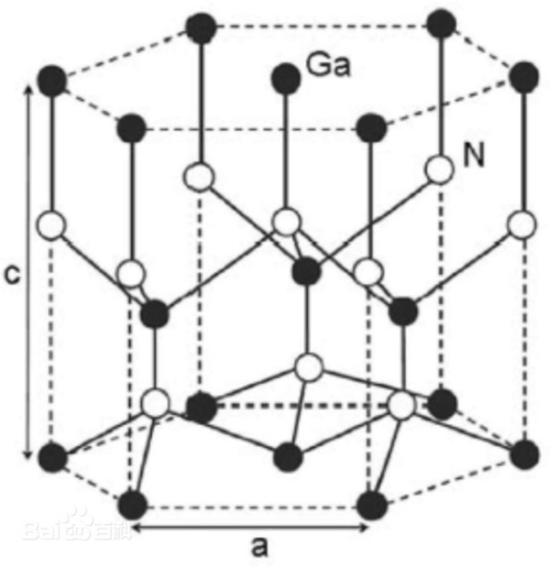
Gallium nitride (GaN) is a semiconductor material with a crystal structure consisting of a lattice of gallium and nitrogen atoms. Gallium nitride crystals have a cubic crystal system structure, and their cells contain an arrangement of atoms with a hexagonal close-packed structure.
The lattice structure of gallium nitride crystals can be described as each gallium atom is surrounded by four nitrogen atoms, and four gallium atoms also surround each nitrogen atom. This structure is known as the sphalerite structure or the helical alkene structure, which consists of an alternating arrangement of covalent and ionic bonds formed by gallium and nitrogen atoms.
In the structure of gallium nitride, the nitrogen atoms form covalent bonds with the surrounding gallium atoms, and these covalent bonds give the crystal a stable structure. At the same time, the nitrogen atoms accept electrons from the gallium atoms, forming positive and negative ions in the gallium nitride crystal. This combination of covalent and ionic bonds gives gallium nitride good electron mobility and optical properties.
In addition, the lattice in gallium nitride crystals often contains impurity atoms, such as silicon and carbon, etc. The doping of these impurity atoms can modulate the electrical and optical properties of gallium nitride, making it suitable for different applications.
Fig. 5 Crystal Structure of Gallium Nitride
4.2 Properties of Gallium Nitride
GaN is an extremely stable compound and a hard, high melting point material with a melting point of about 1700°C. GaN has a high degree of ionization, which is the highest among III-V compounds (0.5 or 0.43). At atmospheric pressure, GaN crystals generally have a hexagonal fibrillated zincite structure. It has four atoms in a protocell with an atomic volume about half that of GaAs. Because of its hardness, it is another good material for coating protection.
Energy Gap and Electronic Structure: Gallium nitride's wider energy gap (about 3.4 eV) gives it high transparency in the visible region, which is critical for optoelectronic devices such as LEDs and lasers. Its direct bandgap properties mean that the conservation of energy and momentum holds when electrons jump, which helps improve the efficiency of optoelectronic devices. GaN's electronic structure also determines its electron mobility and carrier transport properties, which are critical to the speed and power characteristics of the device.
Mechanical Properties: Gallium nitride has a high hardness, close to that of sapphire (about 9 on the Mohs hardness scale), which makes it resistant to a certain degree of mechanical stress and scratches. Its high modulus of elasticity makes Gallium Nitride more resilient and stable in applications, able to withstand a certain degree of external pressure and strain.
Thermal Properties: Gallium nitride has excellent thermal conductivity, which is high relative to other semiconductor materials. This high thermal conductivity allows Gallium Nitride devices to effectively dissipate heat during operation, reducing temperature gradients and improving device performance and reliability. In addition, Gallium Nitride's relatively small coefficient of thermal expansion means that it is less susceptible to dimensional changes and deformation during temperature changes, helping to maintain the structural stability of the device.
Optical Properties: Gallium nitride has high transparency and a low absorption coefficient in the visible region, which allows it to achieve efficient energy conversion in optoelectronic devices such as LEDs and lasers. Its high refractive index allows Gallium Nitride to achieve efficient optical coupling, thereby increasing the luminous efficiency and output power of optoelectronic devices.
Chemical Stability: Gallium nitride has good chemical stability and is resistant to many common chemical corrosion and oxidation reactions, such as acids, alkalis, and solvents. This enables Gallium Nitride to maintain stable performance in a variety of harsh environmental conditions, such as high temperature, high humidity, and corrosive gas environments.
Electronic Performance: Gallium nitride has excellent electron mobility, typically in the range of several hundred to several thousand cm2/(V-s), which gives it excellent performance in high-frequency and high-power electronics. Its high electron mobility and high saturation drift rate allow Gallium Nitride devices to have low on-resistance and high switching speeds for high-speed, high-frequency application scenarios.
4.3 Preparation of Gallium Nitride
The growth of GaN material is realized by the chemical reaction between Ga decomposed from TMGa and NH3 at high temperature, with the reversible reaction equation:
Ga+NH3=GaN+3/2H2
Growing GaN requires a certain growth temperature and a certain partial pressure of NH3. The methods that people usually use are conventional MOCVD (including APMOCVD, and LPMOCVD), plasma-enhanced MOCVD (PE-MOCVD), and electron cyclotron resonance-assisted MBE. The required temperature and NH3 partial pressure are sequentially reduced. A study indicated that the equipment used was AP-MOCVD with a horizontal reactor and special design modifications, using domestically produced high-purity TMGa and NH3 as source program materials, DeZn as P-type doping source, (0001) sapphire with (111) silicon as substrate using high-frequency inductance heating, low-resistance silicon as the heat generator, and high-purity H2 as the carrying gas for the MO source. High-purity N2 was used as the conditioning of the growth zone. HALL measurements, bicrystal diffraction, and room temperature PL spectroscopy were used as a qualitative characterization of GaN.
4.4 Applications of Gallium Nitride
1. New electronic devices
GaN material series with low heat generation rate and high breakdown electric field is an important material for the development of high-temperature high-power electronic devices and high-frequency microwave devices. At present, with the progress of MBE technology in the application of GaN materials and the breakthrough of key thin film growth technology, a variety of GaN heterostructures have been successfully grown. New types of devices such as metal field effect transistors (MESFETs), heterojunction field effect transistors (HFETs), modulation doped field effect transistors (MODFETs), etc., have been prepared from GaN materials. Modulation-doped AlGaN/GaN structure has a high electron mobility (2000cm2/v-s), high saturation velocity (1 × 107cm/s), and low dielectric constant, is the production of microwave devices of priority materials; GaN wider forbidden bandwidth (3.4eV) and sapphire and other materials for the substrate, heat dissipation performance is good, conducive to the device work in high-power conditions.
2. Optoelectronic devices
GaN material series is an ideal material for short-wavelength light-emitting devices, and the bandgap of GaN and its alloys covers the spectral range from red to ultraviolet. Since the development of homojunction GaN blue LEDs in Japan in 1991, InGaN/AlGaN dual heterojunction ultra-bright blue LEDs and InGaN single quantum well GaNLEDs have been introduced. At present, Zcd and 6cd single quantum well GaN blue and green LEDs have entered the stage of mass production, thus filling the gap of blue LEDs on the market for many years. Blue light-emitting devices have a huge application market in the fields of information access of high-density optical disks, all-optical displays, and laser printers. With the Ⅲ nitride materials and devices research and development work continuing to deepen, GaInN ultra-high blue and green LED technology has been commercialized, and now the world's major companies and research institutes have invested heavily in joining the ranks of the competition to develop blue LED.
3. Sensors
Gallium Nitride can be used to make highly accurate and sensitive pressure sensors. The electrical properties of Gallium Nitride change when pressure is applied externally, and pressure can be measured by measuring parameters such as its resistance, capacitance, or field effect. The thermal properties of Gallium Nitride materials make them suitable for manufacturing high-temperature sensors. Gallium nitride has excellent stability and thermal conductivity in high-temperature environments and can be used to manufacture high-temperature sensors, such as automotive engine temperature sensors and high-temperature process monitoring sensors. It can also be used to manufacture gas sensors. The surface of gallium nitride has good chemical inertness and can have specific chemical reactions with many gases, so it can be used to detect the concentration of specific gases, such as nitrogen oxides, ammonia, and so on, using its surface chemical properties. Due to the excellent optical properties of gallium nitride, its application in optical sensors can realize high-precision measurements of parameters such as light intensity, wavelength, and direction. Through specific modification of biomolecules with the surface of Gallium Nitride materials, high sensitivity and high selectivity detection of biomolecules, such as DNA, proteins, cells, etc., can be realized.

Fig. 6 Applications of Gallium Nitride
5 Conclusion
Gallium-based compounds, including Ga2O3, GaAs, and GaN, represent a cornerstone of modern semiconductor technology due to their remarkable electrical, optical, and thermal properties. Each material possesses unique strengths: Ga2O3 excels in high-power and high-voltage applications with its ultra-wide bandgap and high breakdown electric field, GaAs remains a leading material for high-speed and optoelectronic devices owing to its high electron mobility and direct bandgap. At the same time, GaN has transformed power electronics and high-frequency communication systems with its robustness, efficiency, and wide operational range.
Developing advanced synthesis techniques, such as chemical vapor deposition, molecular beam epitaxy, and other tailored fabrication methods, has enabled precise control over material quality, paving the way for innovative applications across industries. From power conversion and ultraviolet detection to 5G communication and renewable energy systems, gallium compounds are driving technological progress and addressing the growing demand for energy-efficient, high-performance devices.
As research and development continue, these materials are expected to overcome existing challenges, such as thermal management and scalability, through material engineering and integration with emerging technologies. Gallium-based compounds will remain at the forefront of innovation, underpinning future advancements in electronics, optoelectronics, and beyond.
Stanford Advanced Materials (SAM) is a key provider of high-quality germanium materials, supporting these critical applications with reliable material solutions.
Further Reading:
Essential Electronic Materials: Part 1 - Silicon

