Essential Electronic Materials: Part 5 - Carbon-Based Materials
1 Introduction
Carbon-based materials have emerged as transformative elements in electronic materials due to their extraordinary physical, chemical, and electronic properties. Graphene, carbon nanotubes (CNTs), and fullerenes stand out as versatile materials with applications ranging from high-speed transistors to advanced energy storage devices. Graphene's remarkable conductivity and mechanical strength, CNTs' unique one-dimensional structure and flexibility, and fullerenes' distinct molecular configuration and semiconductor characteristics have collectively positioned them as pivotal components in modern electronics. This article explores these materials, delving into their principles, advantages, and real-world applications in electronic devices, illustrating how carbon redefines the possibilities in electronics and technology.
2 Graphene
Graphene is an allotrope of carbon in which carbon atoms are bonded in sp² hybridization to form a single hexagonal honeycomb lattice graphene layer. Fullerenes (C60), graphene quantum dots, carbon nanotubes, nanoribbons, multi-walled carbon nanotubes, and nano horns can be constructed using this crystalline structure of graphene. Stacked layers of graphene (greater than 10 layers) form graphite, with the layers held together by van der Waals forces and a crystal plane spacing of 0.335 nanometers. Graphene has excellent optical, electrical, and mechanical properties, and has important applications in materials science, micro- and nanofabrication, energy, biomedicine, and drug delivery, and is considered a revolutionary material for the future.
2.1 Structure and Properties of Graphene
The arrangement of carbon atoms inside graphene is bonded with sp2 hybridized orbitals as in graphite monatomic layers and has the following characteristics: carbon atoms have four valence electrons, three of which generate sp2 bonds, i.e., each carbon atom contributes a non-bonded electron located in the pz orbitals, the pz orbitals of the near-neighboring atoms are oriented perpendicularly to the plane can be formed into a π-bond, the newly formed π-bonds are semi-filled state. The study confirms that the coordination number of carbon atoms in graphene is 3, the bond length between every two neighboring carbon atoms is 1.42 × 10⁻¹⁰ m, and the angle between the bond and the bond is 120°. In addition to the σ-bonds linking with other carbon atoms to form a honeycomb layer structure of a hexagonal ring, the pz orbitals perpendicular to the plane of the layer of each carbon atom can form large π-bonds with multiple atoms running through the entire layer (similar to benzene rings), resulting in excellent electrical conductivity and optical properties.
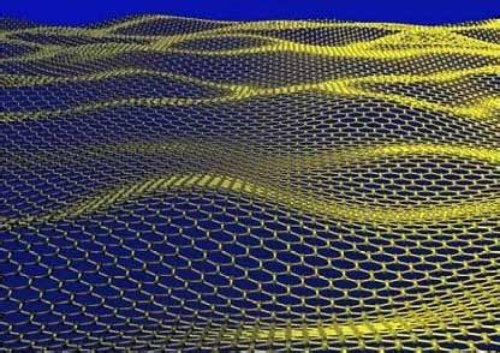
Fig. 1 Graphene Is a Single-Layer Structure of Carbon Atoms
Graphene has a carrier mobility of about 15,000 cm2/(V-s) at room temperature, a value more than 10 times that of silicon, and more than twice that of indium antimonide (InSb), the substance with the highest known carrier mobility. Under certain specific conditions such as low temperatures, graphene's carrier mobility can even be as high as 250,000 cm2/(V-s). Unlike many materials, graphene's electron mobility is less affected by temperature changes, and the electron mobility of single-layer graphene is around 15,000cm2/(V-s) at any temperature between 50 and 500K.
In addition, the half-integer quantum Hall effect of electron carriers and hole carriers in graphene can be observed by changing the chemical potential through the action of an electric field, and scientists have observed this quantum Hall effect in graphene at room temperature. The carriers in graphene follow a special quantum tunneling effect and do not backscatter when they encounter impurities, which is the reason for graphene's local superconductivity as well as its very high carrier mobility. Neither electrons nor photons in graphene have rest mass; their velocity is a constant that has no relation to kinetic energy.
Graphene is a zero-range semiconductor because its conduction and valence bands meet at the Dirac point. The Brillouin zone, the edge of momentum space at the six positions of the Dirac point, is divided into two sets of equivalent triplets. In contrast, conventional semiconductors typically have Γ as their major point with zero momentum.
2.2 Applications of Graphene
Integrated Circuits: Graphene has great potential in the field of integrated circuits due to its excellent electrical and thermal conductivity. For example, IBM has successfully developed integrated circuits made of graphene wafers that work as broadband RF mixers up to 10 GHz. In addition, graphene has been used in the fabrication of 3D integrated circuits to solve heat dissipation and electromagnetic interference problems.
Field Effect Transistors (FETs): Graphene FETs are ideally suited as channel materials due to their high carrier mobility and atomic thickness. Graphene FETs are used in both analog and digital circuits. In analog circuits, graphene FETs can be used for RF applications; in digital circuits, methods such as chemical doping can open up the bandgap of graphene and improve its switching current ratio, thus enhancing its potential for use in digital logic devices.
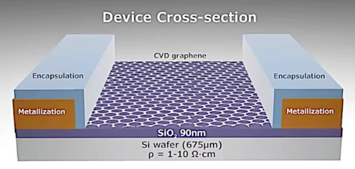
Fig. 2 Graphene Field Effect Transistor (GFET) Construction
Organic Light Emitting Diode (OLED): Graphene is used as a transparent conductive electrode for OLEDs, replacing the traditional ITO material due to its light transmission and conductivity. OLED devices with graphene electrodes are comparable to ITO electrodes in terms of optical and mechanical properties, and graphene is better flexible, which is conducive to the manufacture of bendable display devices.
Chemical Sensors: Graphene's high specific surface area and sensitivity to the environment give it great potential in the field of chemical sensors. Graphene chemical sensors can be used to detect various gases such as NO2 and NH3 with high sensitivity and low detection limits.
Optoelectronic Devices: Graphene shows great potential in the field of optoelectronic devices due to its unique physicochemical properties. Its advantages include high electrical conductivity, broad spectral absorption, ultra-fast carrier mobility, and good mechanical flexibility. Graphene's broad spectral absorption properties and fast electronic dynamics enable efficient detection from the ultraviolet to the far infrared in photodetectors and are suitable for high-speed fiber optic communications and terahertz detection. As a transparent conductive material, graphene is widely used in organic solar cells and chalcogenide solar cells to enhance photovoltaic conversion efficiency and support flexible, wearable devices. It can also be used as a transparent anode in light-emitting diodes or combined with other materials to enhance luminescent properties for flexible displays and OLED devices. In addition, graphene is widely used in optical modulators and ultrafast lasers due to its high nonlinear optical response, enabling efficient optical signal modulation and ultrashort pulse laser output. Its flexibility and transparency also support the development of flexible optoelectronic devices such as curved displays and electronic skins.
3 Carbon Nanotubes (CNTs)
Carbon nanotubes, a one-dimensional quantum material with a special structure, have radial dimensions on the order of nanometers and axial dimensions on the order of micrometers, and the tube is essentially sealed at both ends. Carbon nanotubes consist mainly of carbon atoms arranged in a hexagonal pattern to form coaxial circular tubes with several to dozens of layers. The distance between layers is fixed at about 0.34 nm, and the diameter is generally 2-20 nm, and the carbon nanotubes can be categorized into sawtooth, armchair, and spiral according to the different orientations of the carbon hexagons along the axial direction. Among them, the spiral-type carbon nanotubes have chirality, while the serrated and armchair-type carbon nanotubes have no chirality.
3.1 Structure and Properties of Carbon Nanotubes
Carbon atoms in carbon nanotubes are predominantly sp2 hybridized, while the hexagonal lattice structure has a certain degree of bending, forming a spatial topology, which can form certain sp3 hybridized bonds, that is, the formation of chemical bonds at the same time with a mixed hybridization of the sp2 and sp3 state, and these p orbitals overlap each other to form highly exoticized large π-bonds outside of the carbon nanotubes graphene sheet. Large π-bonds on the outer surface of the carbon nanotubes is the large π-bonds on the outer surface of carbon nanotubes are the chemical basis for the non-covalent bonding between carbon nanotubes and some macromolecules with conjugation properties.
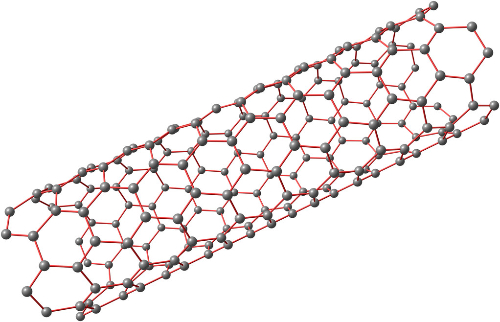
Fig. 3 Structure of Carbon Nanotubes
The results of photoelectron spectroscopy of multi-walled carbon nanotubes show that both single-walled carbon nanotubes and multi-walled carbon nanotubes combine certain functional groups on their surfaces, and the carbon nanotubes obtained by different preparation methods have different surface structures due to the different preparation methods and post-processing processes. Generally speaking, single-walled carbon nanotubes have higher chemical inertness and their surfaces are purer, while the surfaces of multi-walled carbon nanotubes are much more active and incorporate a large number of surface groups, such as carboxyl groups. The results of surface detection of carbon nanotubes by variable angle X-ray electron spectroscopy show that the surface of single-walled carbon nanotubes is chemically inert and the chemical structure is relatively simple, and with the increase of the number of layers of the carbon nanotube wall, the defects and chemical reactivity are enhanced, and the chemical structure of the surface tends to be complicated. The chemical structure of the inner layer of carbon atoms is relatively single, the chemical composition of the outer layer of carbon atoms is more complex, and there is often a large amount of amorphous carbon deposited on the outer layer of carbon atoms. Due to the inhomogeneity of physical and chemical structures, a large number of surface carbon atoms in carbon nanotubes have different surface microenvironments, and therefore also have energetic inhomogeneity.
Carbon nanotubes are not always straight, but have localized areas of convexity and concavity, due to the emergence of pentagons and heptagons during hexagonal preparation. If the pentagon appears exactly at the tip of the carbon nanotube, it forms the seal of the carbon nanotube. When the heptagon appears, the nanotube is concave. These topological defects can change the helical structure of carbon nanotubes, and the electronic energy band structure in the vicinity where the defects appear is also altered. Also, two neighboring carbon nanotubes are not directly glued together but are kept at a distance.
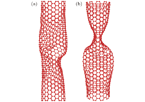
Fig. 4 Buckling instability configuration of carbon nanotubes with polyatomic vacancy defects under axial loading: (a) Carbon nanotubes with polyatomic vacancy defects distributed along the axial direction; (b) carbon nanotubes with polyatomic vacancy defects distributed along the circumferential direction.[1]
The P electrons of carbon atoms on carbon nanotubes form a large range of off-domain π-bonds, and due to the significant conjugation effect, carbon nanotubes have some special electrical properties. For metallic carbon nanotubes, the valence band and the conduction band are partially overlapped, equivalent to a half-full energy band, the electrons can move freely, showing a metal-like conductivity; while semiconducting carbon nanotubes have a small band gap between the valence band and the conduction band, and the valence-band electrons can be jumped to the conduction band at room temperature to conduct electricity.
Carbon nanotubes have good electrical conductivity because the structure of carbon nanotubes is identical to the lamellar structure of graphite. Theory predicts that their electrical conductivity depends on their tube diameter and the helix angle of the tube wall. When the tube diameter of CNTs is larger than 6 nm, the electrical conductivity decreases; when the tube diameter is smaller than 6 nm, CNTs can be viewed as one-dimensional quantum wires with good electrical conductivity. It has been reported that Huang considered carbon nanotubes with a diameter of 0.7 nm to be superconducting by calculations, and although their superconducting transition temperature is only 1.5 × 10⁻⁴ K, it foretells the prospect of carbon nanotubes in the field of superconductivity.
The vector Ch is commonly used to represent the direction of atomic arrangement on carbon nanotubes, where Ch = na1 + ma2, denoted as (n, m). where a1 and a2 denote the two basis vectors, respectively, and (n, m) is closely related to the electrical conductivity of carbon nanotubes. For a given (n, m) nanotube, if there is 2n + m = 3q (q is an integer), then this direction exhibits metallicity and is a good conductor, otherwise it behaves as a semiconductor. For the n = m direction, carbon nanotubes exhibit good electrical conductivity, with conductivity typically up to 10,000 times that of copper.
3.2 Applications of Carbon Nanotubes
EFETs: Carbon nanotubes have excellent electronic conductivity and thermal stability, making them ideal for manufacturing high-performance EFETs. E-field devices, such as picture tubes, fluorescent screens, and micro-lasers, are mainly used in microelectronics and optoelectronics. These properties of carbon nanotubes significantly improve the emission performance of these devices.
Electronic sensors: Carbon nanotubes are also widely used in electronic sensors. Due to their ultra-high sensitivity, they can sense small physical changes in their surroundings and remain stable under extreme conditions such as high temperatures. Carbon nanotubes are gaining attention as a new sensor material, especially in the field of flexible electronics.

Fig. 5 Cobalt-Manganese Oxide Carbon Nanotube Composites for Improved Performance in Sensors
Solar Cells: Carbon nanotubes have also been used in solar cells with remarkable results. Although the specific details are not described in detail in the search results, it can be speculated that their application in photovoltaic effects may enhance the efficiency and stability of solar cells.
4 Fullerenes
Fullerene, a hollow molecule composed entirely of carbon, is spherical, ellipsoidal, columnar, or tubular. Fullerene is structurally similar to graphite, which is made up of layers of graphene stacked with six-membered rings, while fullerene contains not only six-membered rings but also five-membered rings and occasionally seven-membered rings. Depending on the total number of carbon atoms, fullerenes can be categorized as C20, C60, C70, C76, C80, and so on. Among them, the smallest fullerene is C20. The highly symmetric cage-like structure of C60 gives it high stability, and thus it is the most widely studied in the fullerene family.
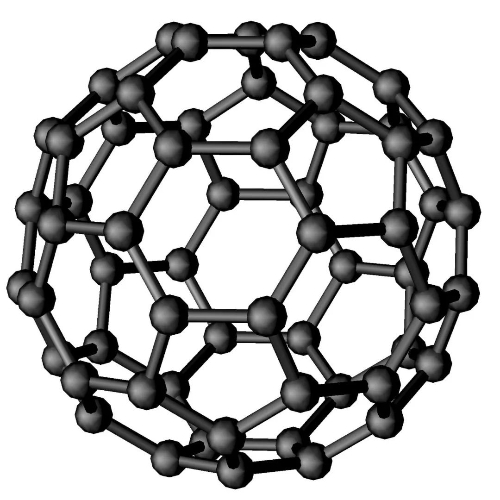
Fig. 6 Structure of Fullerenes
Fullerene is one of the most important carbon-containing nanomaterials in recent years due to its unique zero-dimensional structure. Meanwhile, fullerenes have special optical properties, electrical conductivity, and chemical properties, so fullerenes and their derivatives have been widely used in electricity, light, magnetism, and material science.
4.1 Structure and Properties of Fullerenes
Mathematically, fullerenes are all structured as convex polyhedra with pentagonal and hexagonal faces. The smallest fullerene is C20 with an ortho dodecahedral configuration. There are no fullerenes with 22 vertices, after that, there are all fullerenes with C2n, n=12, 13, 14, etc.The number of pentagons in all fullerene structures is 12 and the number of hexagons is n-10.
After it was possible to produce C60 in large quantities many of its properties were discovered, soon Haddon et al. found that alkali metal-doped C60 had metallic behavior, and in 1991 potassium doped C60 was found to have superconducting behavior at 18 K this is the highest molecular superconducting temperature to date, and after that, a large number of superconducting properties of metal-doped fullerenes were discovered. It was shown that the superconducting transition temperature increases with the cell volume of alkali metal-doped fullerenes. Cesium can form the largest alkali metal ions, so cesium-doped fullerene materials have been widely studied, and the superconducting properties of Cs3C60As at 38 K have been reported recently, though at high pressure. The one with the highest superconducting transition temperature at 33 K at atmospheric pressure is Cs2RbC60. The BCS theory of superconductivity in C60 solids suggests that the superconducting transition temperature increases with increasing cell volume because the spacing between C60 molecules correlates with an increase in the density of states at the Fermi energy level N (εF), and so scientists have done a great deal of work attempting to increase the distances between the fullerene molecules, in particular, by inserting neutral molecules inserted into the A3C60 lattice to increase the spacing while keeping the valence of C60 unchanged. However, this amination technique unexpectedly yielded novel and special properties of the fullerene insertion complexes: the Mott-Hubbard transition and the relationship between the orientation/orbital ordering of the C60 molecules and the magnetic structure. The C60 solid is composed of weakly interacting forces, and is, therefore, a molecular solid and retains the properties of a molecule. The discrete energy levels of a free C60 molecule are only weakly diffuse in the solid, resulting in a narrow non-overlapping band gap in the solid of only 0.5 eV. Undoped C60 solids, with a 5-fold hu band as its HOMO energy level and a 3-fold t1u band as its empty LUMO energy level, this system is band-forbidden. But when the C60 solid is doped with metal atoms, the metal atoms give the t1u band electrons or some of the electrons of the 3x t1g band to occupy and sometimes take on a metallic character. Although its t1u band is partially occupied, according to the BCS theory A4C60's t1u band is partially occupied should have metallic properties, but it is an insulator, this paradox may be explained by the Jahn-Teller effect, where spontaneous deformation of a high symmetry molecule leads to splitting of its concatenated orbitals thus gaining electronic energy. This Jahn-Teller type of electron-phonon interaction is so strong in C60 solids that it can disrupt the valence band pattern of a particular valence state. Narrowband gaps or strong electron interactions and a condensed ground state are important to understand and explain the superconductivity of fullerene solids. The simple Mott-Hubbard model produces insulating localized electronic ground states when the electronic mutual repulsion is larger than the bandwidth, which explains the absence of superconductivity in cesium-doped C60 solids at atmospheric pressure. The localization of t1u electrons driven by electronic interactions beyond a critical point generates Mott insulators, and the use of high pressure reduces the spacing of fullerenes from each other, at which point the cesium-doped C60 solid exhibits metallicity and superconductivity.
There is no complete theory on the superconductivity of C60 solids, but the BCS theory is widely accepted because strong electron interactions and Jahn-Teller electron-phonon couplings can produce electron pairs that give high insulator-metal transition temperatures.
4.2 Applications of Fullerenes
Capacitors: Fullerenes have important applications in the manufacture of high-performance capacitors due to their good electrical conductivity and chemical stability. Its unique molecular structure significantly improves the conductivity and energy storage density of the electrodes, while enhancing the cycle life and reliability of the capacitors. Fullerene-enhanced supercapacitors are capable of storing and releasing large amounts of electricity in a short period with stable and efficient performance and are widely used in electronic devices and energy management systems, providing a high-quality solution for modern energy storage.
Conductive Adhesive: Fullerenes can be used to prepare conductive adhesives with excellent performance, which play an important role in the fixing and connection of electronic components. It provides efficient electron transport paths and significantly improves conductivity. Compared with traditional conductive adhesives, fullerene conductive adhesives have higher viscosity and fluidity while maintaining excellent adhesion, which is suitable for the assembly of precision electronic devices such as chip packages, flexible circuit connections, etc., and meets the demand for high-reliability conductive adhesive applications.
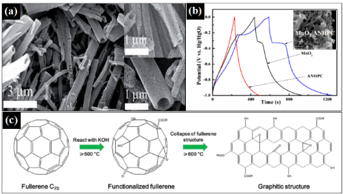
Fig. 7 Application of FMNSs in supercapacitors. (a) SEM image of C60 μm tubes obtained by high-temperature carbonization; (b) charge-discharge curves of fullerene/MnO2 composites (inset shows the SEM image of the composites); (c) charge-discharge curves of C70 μm tubes obtained by KOH activation (inset shows the SEM image of the porous material).
Optoelectronic applications: Fullerene, a key material in optoelectronic devices, exhibits excellent electron acceptor properties and n-type semiconductor performance. Its low carrier complex probability and high electron mobility make it an ideal material for electron transport. Fullerene molecules (e.g., C60 or C70) can be coupled with p-type organic semiconductor materials to effectively improve the charge separation efficiency and performance stability of the devices, which are widely used in organic photovoltaics (OPV), organic field effect transistors (OFETs) and photodetectors. In OPVs, fullerenes act as electron acceptors to enhance the photoelectric conversion efficiency; in OFETs, their transistors show excellent performance in inert environments and are suitable for display drivers and photodetectors; in addition, fullerenes enhance the electron injection and current transfer capabilities of light-emitting diodes (OLEDs), providing technical support for the development of high-efficiency optoelectronic devices.
5 Conclusion
The exploration of graphene, carbon nanotubes, and fullerenes underscores the vast potential of carbon-based materials in shaping the future of electronics. Their unique properties—whether it is graphene's unparalleled conductivity, CNTs' exceptional flexibility, and tensile strength, or fullerenes' distinctive electronic and photonic behavior—have enabled breakthroughs across diverse applications such as transistors, sensors, capacitors, and light-emitting devices. As research and manufacturing technologies continue to advance, these materials promise to overcome existing challenges, paving the way for a new era of innovative, efficient, and sustainable electronic systems. Their integration into cutting-edge technologies will undoubtedly drive progress in fields ranging from renewable energy to next-generation computing, solidifying the essential role of carbon in the evolution of modern electronics.
Stanford Advanced Materials (SAM) is a key provider of high-quality Carbon-Based Materials, supporting these critical applications with reliable material solutions.
Reference
[1] Wang Lei, Zhang Ran-Ran, Fang Wei. Simulation of static and dynamic mechanical characteristics of carbon nanotubes and carbon nano-peapods with defects. Acta Phys. Sin., 2019, 68(16): 166101. doi: 10.7498/aps.68.20190594
[2] [1] Xu T, Shen W, Huang W, et al.Fullerene Micro/Nanostructures: Controlled Synthesis and Energy Applications[J].Materials Today Nano, 2020.DOI:10.1016/j.mtnano.2020.100081.
Related Reading:


