
This year, Stanford Advanced Materials (SAM) focused on encouraging innovation in spherical powder technology. We invited students to share their research proposals, projects, or studies on the applications, challenges, and advancements in this field.
Over the past few months, we received many impressive submissions from students across the United States. After careful consideration, we are pleased to announce the winner of the 2024 Stanford Advanced Materials College Scholarship:
Tucker Erbeck
University of Southern California
Chemical Engineering, Junior
Tucker's research on using spherical powder technology in thin film deposition for semiconductor manufacturing stood out for its creativity and potential impact.
We want to thank all the students who submitted their work. Your ideas and efforts are truly inspiring, and we wish you all the best in your future endeavors.
For more details on our scholarship program and future opportunities, please visit our Scholarship Page.
Winning Project:
Title: Development and Application of Spherical Powder Technology in Thin Film Deposition
Abstract:
The development and application of spherical powder technology in thin film deposition offers a significant advancement in the field of semiconductor manufacturing. This research investigates the impact of using spherical powder targets, produced through high-temperature remelting spheroidization (HRS), compared to traditional solid plate targets in the sputtering deposition process. By optimizing the composition, structure, and deposition techniques of thin films with spherical powders, the study aims to enhance uniformity and quality, leading to notable improvements in semiconductor yield. The experiment involves a systematic comparison of thin films deposited with spherical powders versus solid plates, with controlled parameters such as pressure, target-to-substrate distance, and deposition time. The quality of the films is assessed using scanning electron microscopy (SEM) to analyze grain size, orientation, and defect density. Scholarly research suggests that spherical powders offer improved surface interaction and packing density, resulting in superior film quality with fewer defects. These advancements have the potential to meet the increasing demand for high-performance semiconductor materials and contribute to the future of semiconductor technology through manufacturing efficiency and product performance.
Background:
Deposition involves the addition of extremely thin layers of material onto a substrate from a metal source. Thin film material can be deposited onto a substrate through numerous methods, such as physical vapor deposition (PVD), chemical vapor deposition (CVD), and atomic layer deposition (ALD) [1].
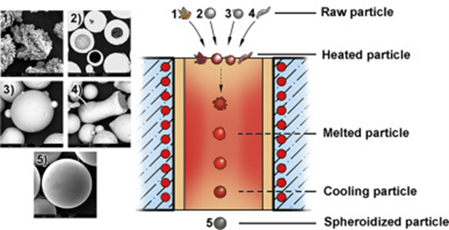
Figure 1: (left) Microscopic morphologies of copper atom throughout high-temperature remelting spheroidization process, (right) Schematic of spheroidization using HRS technology [4].
Sputtering, a type of physical vapor deposition, involves the ejection of high-energy ions onto a target material, causing atoms to be released and deposited onto a substrate. This method is particularly well-suited for large-scale semiconductor manufacturing due to its affordability and ability to deposit over large areas [2].
The properties of the sputtering target heavily influence the quality of thin films. Traditionally, sputtering targets take the form of a solid plate or disk, but recent advancements have enabled the use of spherical powder technology in this process [3]. Spherical powder targets can be prepared via high-temperature remelting spheroidization (HRS), in which metal particles are heated at temperatures well above their temperature points, causing particles to melt and fuse. These heated particles then undergo spheroidization, in which they are rapidly cooled and solidify into spherical shapes. Figure 1 illustrates the entire HRS process, including the rapid heating and cooling process, as well as the effect on the particle shape [4].
HRS ensures that powder targets are spherical, resulting in improvements in thin film uniformity and density [2].
Methodology:
This experiment will be designed to determine the difference in thin film quality between spherical powder and solid plate targets in the sputtering deposition process. Key parameters such as pressure and target-to-substrate difference must be controlled to determine the thin film quality between the two sputtering techniques [5]. In addition, substrate pre-treatment, such as substrate cleaning, must be held constant to ensure that the deposition between the two techniques is as consistent as possible [6].
During the deposition process, deposition time will be held constant for both sputtering methods, allowing for easier comparison in thickness and uniformity of films. In addition, growth rates between the two techniques will be consistent and optimized using thickness-measuring techniques, such as ellipsometry [6].
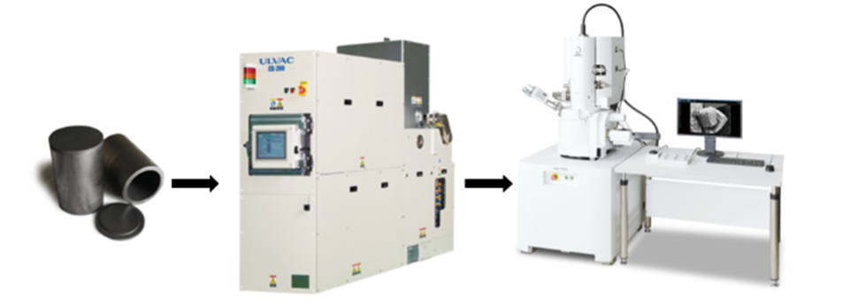
Figure 2: Thin film quality test including: creation of targets with spherical powders and thin disks, deposition of materials via sputtering machine, and material characterization via scanning electron microscope (SEM) [7][8][9]
To enhance the reliability of the results, multiple spherical powders and solid disks will be used in the experiment. This approach increases statistical reliability by providing more data points, ensuring reproducibility across different samples, and evaluating consistency and uniformity in the sputtering process.
The results of the sputtering processes will be analyzed using scanning electron microscopy (SEM). SEM techniques will characterize the materials' microstructure and determine the quality of the deposited thin films [4].
Results:
Understanding the results of the microstructure characterization requires analyzing both grain size and orientation. Using an SEM machine, the size of individual grains within the thin film can be analyzed and compared between the spherical powders and traditional solid plates. Figure 3 depicts an SEM image of the cross section of a multi-layer thin film.
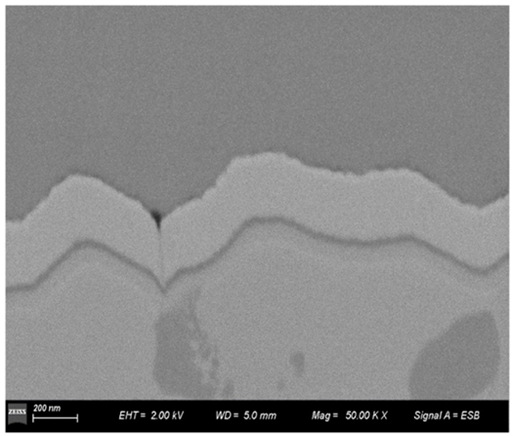
Figure 3: Scanning Electron Microscopy (SEM) image of multi-layer thin film of solar panel captured at 50k× magnification using the Zeiss Auriga FIB-SEM system [10]
This image was taken with an electron high tension (EHT) of 2.00 kV, indicating the acceleration voltage used in the SEM, as well as a distance between the sample and electron gun at 5.0 mm at a magnification of 50,000x [10].
Information about the sample’s microstructure and grain boundaries can be derived at this magnification, helping determine the quality of the thin film. In Figure 3, the grain boundaries are noticeable due to the distinct interfaces between the materials. A smooth interface indicates that the target material had strong adhesion to the substrate during the deposition process.
In addition, SEM analysis of spherical powder and solid-based thin films can reveal important information about potential defects in the thin film. Dark spots or areas that are less dense than the rest of the film might be indicative of defects that arose during the deposition process.
By analyzing thin films through Scanning Electron Microscopy (SEM), spherical powder technologies are expected to produce positive results. The smooth boundaries observed in these films can be attributed to enhanced adhesion properties, which are inherent to spherical powder targets. This is likely due to the improved surface interaction and uniform deposition afforded by the spherical shape of the powders. Furthermore, the increased packing density of spherical powders is expected to reduce the occurrence of defects, contributing to the overall quality and consistency of the thin films. This makes spherical powders a promising material for applications requiring high precision and uniformity in thin film deposition [5].
Potential Implications:
High-quality thin films are crucial for the performance and reliability of advanced processors and memory devices [11]. Spherical powder innovations will help ensure that high-quality thin films will meet global and domestic semiconductor demands.
Thin film quality has implications in many industries. For example, the market demand for semiconductors in the electric vehicles (EV) industry, for example is expected to expand from 2.33 billion to 8.3 billion dollars between 2024-2029.

Figure 4: Increasing market demand for semiconductors in the electric vehicle (EV) market from 2020-2029 [12].
Spherical powder-based deposition will increase the quality of semiconductors, making it easier to meet increasing demand. The uniformity and precision offered by spherical powders ensure that the thin films produced are of the highest quality, which is essential for advanced semiconductor applications [5].
Moreover, spherical powder technology promises to bolster the resilience and security of the semiconductor supply chain. The disruptions experienced during the COVID-19 pandemic, which significantly impacted the production of battery-electric vehicles (BEVs) due to semiconductor shortages, underscore the importance of a stable and efficient supply chain [13]. Improving yield is central to overcoming supply chain issues: a 2018 case study by McKinsey & Company found that a major semiconductor was losing almost $68 million due to yield losses across the eight major steps of its semiconductor production process [14].
By improving the yield and consistency of functional chips, spherical powder technology not only addresses current supply chain challenges but also supports future technological advancements and industry growth. As such, this technology represents a crucial step toward ensuring a robust and reliable supply of high-performance electronic materials for the future [5].
Biography:
Tucker Erbeck is a Junior studying Chemical Engineering with an emphasis on Materials Science at the University of Southern California. He recently completed an internship with California DREAMS at the John O’Brian Nanofabrication Laboratory, where he received comprehensive training in microelectronic fabrication, including thin film technologies. Tucker aspires to become a materials scientist, with a focus on developing novel that enhances the performance and energy efficiency of the next generation of semiconductors.
Works Cited
[1]E. Chen, https://www.mrsec.harvard.edu/education/ap298r2004/Erli%20chenFabrication%20II%20-%20Deposition-1.pdf
[2]“Overview of Spherical Powders | Additive Manufacturing Material,” am-material.com, Oct. 27, 2023.https://am-material.com/news/spherical-powders-a-complete-guide/
[3]F. M. Mwema, E. T. Akinlabi, O. P. Oladijo, and A. D. Baruwa, “Advances in Powder-based Technologies for Production of High-Performance Sputtering Targets,” Materials Performance and Characterization, vol. 9, no. 4, pp. 528–542, Sep. 2020, doi: https://doi.org/10.1520/mpc20190160.
[4]Q. Bao, Y. Yang, X. Wen, L. Guo, and Z. Guo, “The preparation of spherical metal powders using the high-temperature remelting spheroidization technology,” Materials & Design, vol. 199, p. 109382, Feb. 2021, doi: https://doi.org/10.1016/j.matdes.2020.109382.
[5]S. Yu, Y. Zhao, G. Zhao, Q. Liu, B. Yao, and H. Liu, “Review on preparation technology and properties of spherical powders,” The International Journal of Advanced Manufacturing Technology, vol. 132, no. 3–4, pp. 1053–1069, Mar. 2024, doi: https://doi.org/10.1007/s00170-024-13442-w.
[6]C. Linke, “Linking Target Microstructure with its Sputter Performance,” Annual Technical Conference Proceedings, vol. 60, Apr. 2018, doi:https://doi.org/10.14332/svc17.proc.42840.
[7]“Sputtering System CS-200 - ULVAC Vietnam Representative Office,” ULVAC Vietnam Representative Office, Sep. 09, 2021. https://ulvac.com.vn/en/product/vacuum-equipments/sputtering-system/cs-200-series/ (accessed Aug. 30, 2024).
[8]“Scanning Electron Microscope (SEM) | Products | JEOL Ltd.,” Scanning Electron Microscope (SEM) | Products | JEOL Ltd. https://www.jeol.com/products/scientific/sem/
[9]Pyrolytic Graphite Crucible, “Pyrolytic Graphite Crucible | Stanford Advanced Materials,” Global Supplier of Sputtering Targets and Evaporation Materials | Stanford Advanced Materials, Aug. 20, 2018. https://www.sputtertargets.net/pyrolytic-graphite-crucible.html (accessed Aug. 30, 2024).
[10]W. Sun, F. Duan, J. Zhu, M. Yang, and Y. Wang, “An Edge Detection Algorithm for SEM Images of Multilayer Thin Films,” Coatings, vol. 14, no. 3, p. 313, Mar. 2024, doi: https://doi.org/10.3390/coatings14030313.