How was Hafnium Discovered
The Discovery of Hafnium
In 1923, Swedish chemist Hervey and Dutch physicist D. Coster discovered the element hafnium in zircons produced in Norway and Greenland. It was named hafnium. It came from the Latin name Hafnia in Copenhagen. In 1925, Hervey and Coster separated zirconium and titanium by fractional crystallization of fluorinated complexes to obtain pure hafnium salts, and reduced hafnium salts with sodium metal to obtain pure metal hafnium. Hervsi made several samples of pure hafnium.

In 1998, Professor Carl Collins of the University of Texas, in an experiment, claimed that Hf 178m2 irradiated by gamma rays could release enormous amounts of energy, five orders of magnitude higher than a chemical reaction, but three orders of magnitude lower than a nuclear reaction. Hf 178 M2 has the longest life in similar long-lived isotopes: the half-life of Hf 178 M2 is 31 years, so it's natural radioactivity is about 1.6 trillion becquerels. Collins reports that a gram of pure Hf178m2 contains about 1330 megajoules, which is equivalent to the energy released by the explosion of 300 kilograms of TNT.
Collins reports that all the energy in this reaction is released in the form of X-ray or gamma-ray, which is very fast, and Hf178m2 reacts at very low concentrations. The Pentagon has allocated funds for this purpose. The signal-to-noise ratio in the experiment was very low, and since then, no scientist has been able to achieve this reaction under the conditions claimed by Collins, despite numerous experiments by scientists from various organizations, including DARPA and JASON Defense Advisory Group, and Collins has failed to provide strong evidence of its existence. In 2006, Collins proposed the use of induced gamma-ray emission to release energy from Hf 178m2, but other scientists have proved theoretically impossible. Hf178m2 is widely regarded as an energy source in academia.
The Products and Uses of Hafnium
Because hafnium is easy to transmit electrons, it is of great use. Used as the cathode for X-ray tubes, HF and w or Mo alloys are used as electrodes for high voltage discharge tubes. Cathode and tungsten filament manufacturing industry commonly used as X-rays. Pure hafnium is an important material in the atomic energy industry due to its plasticity, easy processing, high-temperature resistance, and corrosion resistance. Hafnium has a large thermal neutron capture cross-section and is an ideal neutron absorber. It can be used as a control rod and protective device in the nuclear reactor. Hafnium powder can be used as a propeller for rockets. The cathode of the X-ray tube can be manufactured in the electrical industry. Hf-Ta alloy can be used as the front protective layer for rocket nozzles and gliding reentry vehicles. Hf-Ta alloy can be used as a tool for steel and resistant material. Hafnium in heat-resistant alloys is used as an additive element, such as tungsten, molybdenum and Tantalum Alloys, adding hafnium. HfC can be used as an additive for cemented carbide due to its high hardness and high melting point. The melting point of 4TaCHfC is about 4215 C, which is the highest melting point compound. Hafnium can be used as a getter for many inflatable systems. Hafnium getter can remove oxygen and nitrogen in the system without gas. Hafnium is often used as an additive in hydraulic oil to prevent the volatilization of hydraulic oil in high-risk operations. It has a strong anti-volatility, so it is generally used in industrial and medical hydraulic oil.

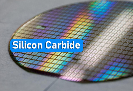
Hafnium elements are also used in the latest intel45 nanometers. Because silicon dioxide (SiO2) is manufacturable and can reduce the thickness to continuously improve transistor performance, processor manufacturers use silica as a gate dielectric material. When Intel introduced the 65-nanometer manufacturing process, the silicon dioxide grid dielectric thickness was reduced to 1.2 nanometers, equivalent to 5-layer atoms. However, as the transistor was reduced to the size of atoms, the difficulty of power consumption and heat dissipation would increase at the same time, resulting in a waste of current and unnecessary thermal energy. Therefore, if we continue to use the current, the current will be reduced. The material, further reducing the thickness of the gate dielectric leakage potential will be significantly increased, reducing transistor technology encounter the limit. In order to solve this key problem, Intel formally proposed to replace silicon dioxide with thicker high-K materials (hafnium-based materials) as the gate dielectric, which also successfully reduced the leakage by more than 10 times. Compared with the previous 65-nanometer technology, Intel's 45-nanometer process has nearly doubled the transistor density, increased the total number of transistors in the processor, or reduced the size of the processor. In addition, transistor switching requires less power, reduced power consumption by nearly 30%, and internal interconnects use copper wires with low-k dielectric.