Exploring the Properties, Manufacturing, and Applications of Gadolinium Gallium Garnet
Introduction
Garnets, which belong to the A3B2(SiO4)3 mineral group, are frequently utilized as gemstones, substrates, and abrasives due to their shared physical properties and crystal structures. Despite their similarities, garnets have variations in chemical composition. In this article, we will delve into the garnet family and specifically focus on gadolinium gallium garnet, providing an overview of its characteristics, manufacturing techniques, and applications. By the end of this article, you will have a fundamental understanding of the properties and uses of gadolinium gallium garnet.
Definition of Gadolinium Gallium Garnet
Gadolinium gallium garnet (Gd3Ga5O12) is a synthesis garnet with impressive thermal, mechanical, and optical properties.
- Gadolinium gallium garnet (GGG) has a high thermal conductivity of 7.4W m-1K-1 and a high melting point of about 1730℃.
- It also stands out with a Mohs hardness of 6.5 to 7.5.
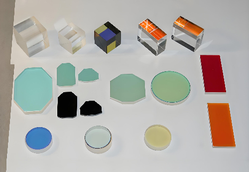
- As for optical features, GGG has an optical loss that is lower than 0.1%/cm. It is transparent enough for optical components between 0.36 and 6.0 μm, while the refractive index of GGG ranges from 2.0 at the UV end to 1.8 at the IR end of the spectrum.
Manufacturing of Gadolinium Gallium Garnet
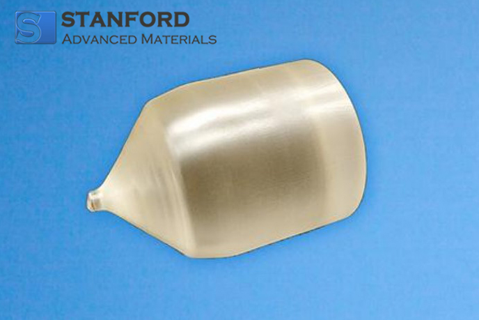
The Czochralski process is a widely used method for manufacturing single crystals, including gadolinium gallium garnet. It was first developed by Jan Czochralski, a Polish scientist, who stumbled upon the method accidentally. While trying to dip his pen in an inkwell, he mistakenly dipped it into a molten tin, and a single tin crystal was formed. This led to the development of the Czochralski process, which has since become the primary method for creating crystals.
Figure 1 shows a schematic diagram of the Czochralski process as applied to the production of silicon crystals.
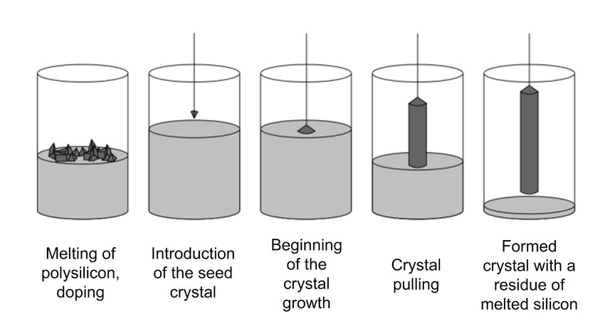
The Czochralski process involves several steps which can be outlined as follows:
First, the material is placed into a round crucible and heated until it reaches a molten state.
Second, a seed crystal is carefully dipped into the molten material and slowly rotated. This allows for the formation of a crystalline structure around the seed.
Finally, the seed crystal is slowly withdrawn from the melt, resulting in the formation of a single crystal at the interface between the seed and the molten material.
Overall, the Czochralski process is a precise and intricate method for creating high-quality single crystals, with each step requiring careful attention and control.
In addition, it is crucial to conduct the Czochralski process in an inert atmosphere to prevent contamination and oxidation. The heating power, rotation rate, and pulling rate must be carefully controlled to achieve the desired crystal shape. Furthermore, dopants can be added to alter the color of the garnet crystal. This technique is frequently used in semiconductor materials, such as silicon and gallium arsenide.
Applications of Gadolinium Gallium Garnet
Gadolinium gallium garnet has a wide range of applications in various industries due to its desirable characteristics. GGG is commonly used as a substrate material for magneto-optical films. For instance, by applying a yttrium iron garnet (YIG) film on a gadolinium gallium garnet substrate, one can create infrared optical isolators. GGG is also used as a substrate material for magnetic bubble memory because its lattice parameter closely matches that of the memory material. Additionally, GGG crystals are essential substrates for microwave isolators.
In the 1970s, GGG was used as a diamond simulant due to its visual similarity to natural diamonds. However, it was quickly replaced by yttrium aluminum garnet (YAG) due to YAG's higher hardness. Nonetheless, GGG remains a popular choice for those seeking a natural diamond appearance in their products.
Other Garnet Materials
Our website offers a variety of synthesized garnets to choose from. One such option is cerium-doped gadolinium aluminum gallium garnet (Ce: GAGG), which is known for its high light yield, fast scintillation response, chemical stability, and excellent energy resolution. Ce:GAGG is an excellent choice for X-ray imaging, computed tomography (CT), and other medical imaging techniques.
Another option is neodymium-doped yttrium aluminum garnet (Nd: YAG), , which has excellent optical absorption and conversion efficiency. Nd:YAG is widely used in laser marking machines, beauty instruments, and cutting machines due to its exceptional properties.

Please visit our homepage for more information.
Related reading: An Introduction to 7 Types of Synthetic Garnet Materials
Conclusion
Gadolinium gallium garnet (GGG) is a highly versatile material widely used as a substrate and gemstone, owing to its exceptional properties such as high melting point, thermal conductivity, hardness, and good optical features. At Stanford Advanced Materials (SAM), we offer high-purity garnets of various diameters to meet your specific requirements. If you are interested, please send us an inquiry and we will be happy to assist you.