Products
- Products
- Categories
- Blog
- Podcast
- Application
- Document
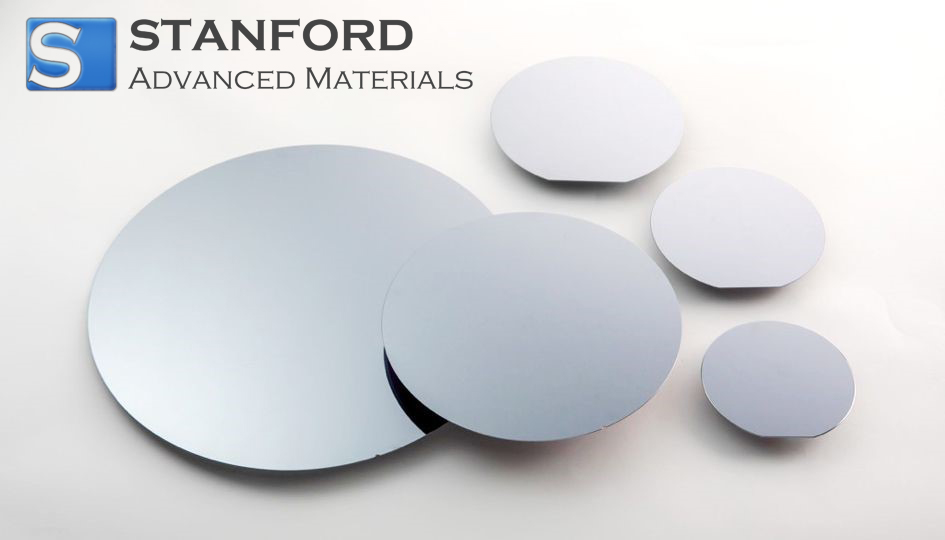
| Catalog No. | CY3307 |
| Substrate Material | SiC |
| Diameter | 4, 5, 6, 8 inch |
| Epi-layer thickness, µm | 0.1-100 |
| Orientation | <100>, <111> |
| Substrate Thickness (um) | 300-725 |
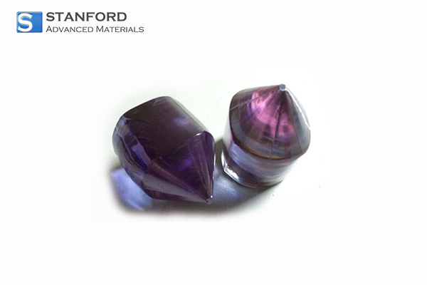
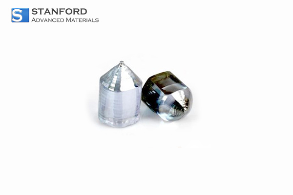
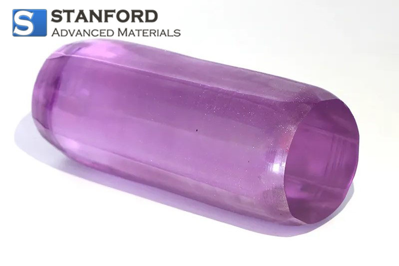
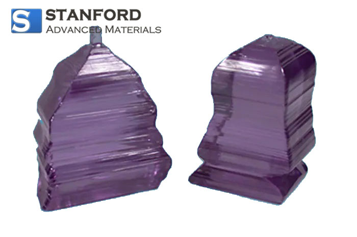
Epitaxial Wafer SiC-GaN EPI refers to a semiconductor thin film grown on a substrate. Stanford Advanced Materials (SAM) has rich experience in manufacturing and supplying high-quality optical products.
Related products: Sapphire Epitaxial Wafer EPI Wafer, SOI Wafer, Silicon Carbide Wafer

Send us an Inquiry now to find out more Information and the latest prices,thanks!
Copyright © 1994-2025 Stanford Advanced Materials owned by Oceania International LLC, All Rights Reserved.