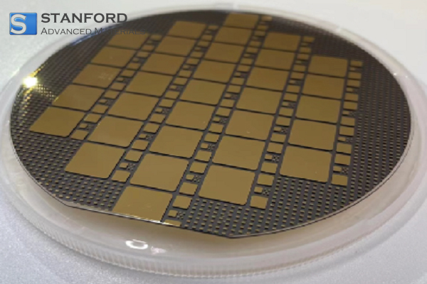
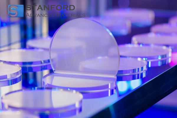
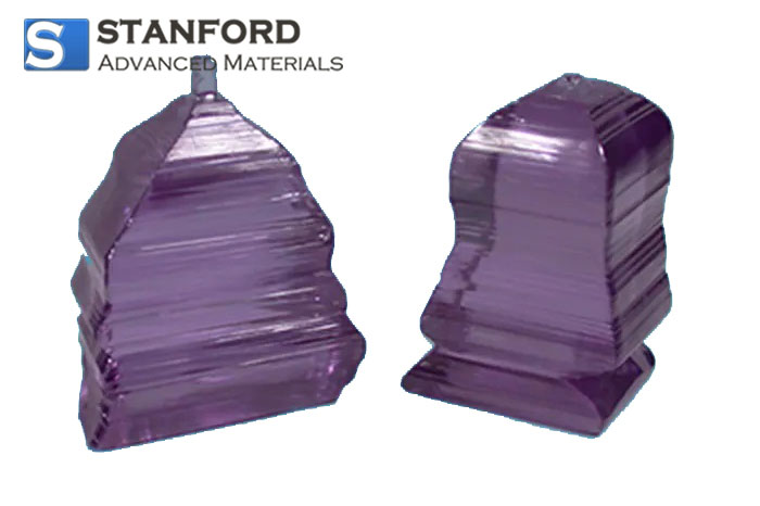
CY4611 Gallium Oxide Wafer
| Catalog No. | CY4611 |
| Material | β-Ga2O3 |
| Grade | Prime Grade |
| Size | Dia. 25.4mm-50.8mm, Length 5mm-15mm, or customized |
| Band gap | 4.8~4.9eV |
| Orientation | <201> <010> |
Gallium Oxide is a wide-bandgap semiconductor material. Stanford Advanced Materials (SAM) has rich experience in manufacturing and supplying high-quality Optical Products.
Related products: Gallium Nitride Wafer, Gallium Phosphide Wafer, Sapphire Wafer, Silicon Wafer
INQUIRY
Add to Inquiry List
Description
Specification
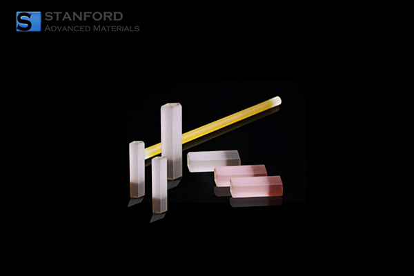
Gallium Oxide Wafer Description
Gallium Oxide Wafer unlike SiC or GaN has high voltage resistance, wide band gap, and low producing cost. Gallium Oxide Wafer is a fourth-generation semiconductor. It is mainly used to power electronic devices such as electric vehicles. There are five crystalline phases of Ga2O3, but beta-Ga2O3 is the only one that can exist stably at high temperatures.
Gallium Oxide Wafer Specifications
|
Grade |
Prime Grade |
|
Size |
D25.4mm-50.8mm, Length 5mm-15mm (Special sizes are available by request) |
|
Band Gap |
4.8~4.9eV |
|
Orientation |
<201> <010> |
|
Electrical Resistivity(300K) |
>1E6 Ohm*cm |
|
Crystal type |
Monoclinic |
|
Dielectric constant |
10 |
|
Density |
5.95/cm3 |
|
Melting Point |
1725℃ |
|
Thickness |
0.5~0.8mm |
|
Polishing |
Epi-ready, RMS < 0.5 nm on Ga face, optical polish on O face |
Gallium Oxide Wafer Applications
Used in high-power electronics.
Used in high-frequency electronics.
Used as the substrate for high electron mobility transistors (HEMT).
Used in UV detectors, LEDs, and gas sensors.
Gallium Oxide Wafer Packaging
Our Gallium Oxide Wafer is carefully handled during storage and transportation to preserve the quality of our product in its original condition.
LATEST RECOMMENDED
CY0104 Magnesium Fluoride Crystal (MgF2 Crystal)
CY0106 Barium Fluoride Crystal
CY0474 Diffusion Bonded Crystals
CY0476 Neodymium-doped Yttrium Orthovanadate (Nd:YVO4)
CY0477 Neodymium-doped Gadolinium Orthovanadate (Nd:GdVO4)
CY0478 Nd:YAG (Neodimium-doped Yttrium Aluminum Garnet)
CY0479 Nd:KGW (Neodymium-doped Potassium-Gadolinium Tungstate Crystal)

CY0481 Ti:Sapphire (Titanium-doped Sapphire Crystal)
GET A QUOTE
Send us an Inquiry now to find out more Information and the latest prices,thanks!