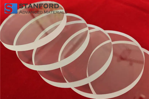
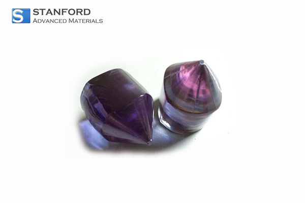
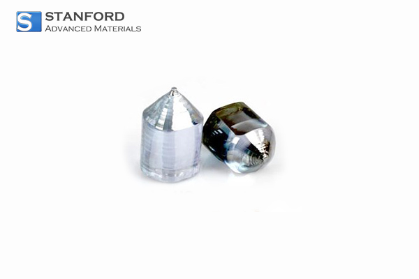
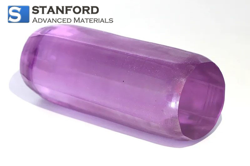
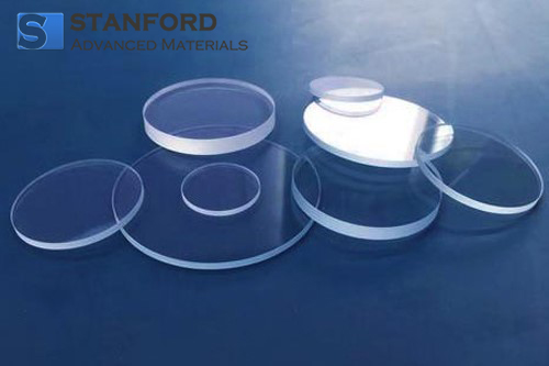
OP5084 CVD Diamond Wafer
| Catalog No. | OP5084 |
| Type | single crystal grains Substrate: SiO2/Si, Quartz, Sapphire, Silicon wafer, PET, etc. |
| Size | 10*10, 15*15, 20*20 (mm) |
| Growth Method | Microwave Plasma Chemical Vapor Deposition (MPCVD) |
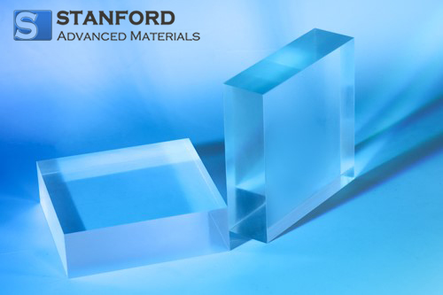
CVD Diamond Wafer is a new material with excellent optical and thermal conductive properties. Stanford Advanced Materials (SAM) has rich experience in manufacturing and supplying high-quality CVD Diamond wafers.
Related products: Lithium Tantalate Wafers, Silicon Carbide Wafer, Infrared Crystal Silicon (Si Crystal), Sapphire Epitaxial Wafer EPI Wafer
INQUIRY
Add to Inquiry List
Description
Specification
CVD Diamond Wafer Description
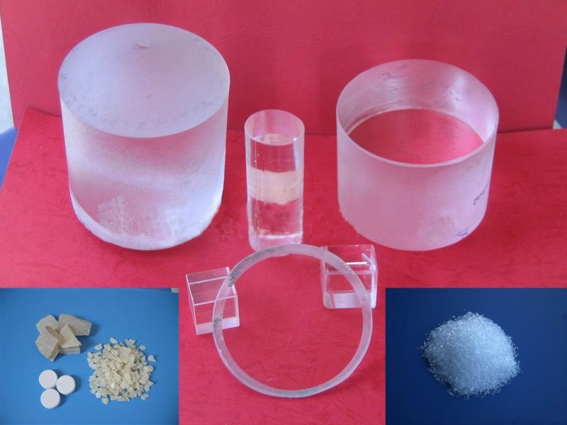
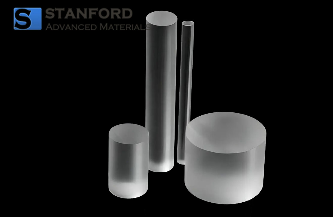
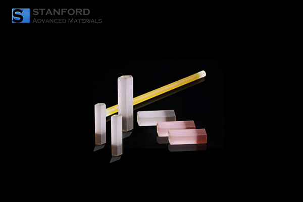
CVD Diamond Wafer has outstanding physical and chemical properties. It has an almost continuous band of optical transparency from UV to THz. Diamond is one type of carbon and has the highest hardness and thermal conductivity at the same time with high wear resistance, chemical inertness, and excellent radiation resistance. CVD Diamond Wafer can be used in multiple band ranges such as X-ray, ultraviolet, infrared, microwave, and so on.
It plays an important role in high energy input, low dielectric loss, high Raman gain, low beam distortion, erosion resistance, and other aspects that can’t be replaced by general optic materials. CVD Diamond Wafers are the best thermal management material for high heat flux devices due to their excellent thermal conductivity.
CVD Diamond Wafer Specifications
|
Grade |
Optical Grade |
Heat Sink Grade |
||
|
- |
Polycrystal |
Monocrystal |
Polycrystal |
Monocrystal |
|
Growth Method |
MPCVD |
MPCVD |
MPCVD |
MPCVD |
|
Size (mm) |
Φ50~Φ150 |
≥8 in light direction |
Φ50~Φ150 |
≥10 |
|
Luminousness (%, 1mm thickness) |
>60%@λ>500nm >70%@λ>10μm |
>65%@λ>500nm >71%@λ>10μm |
/ |
/ |
|
Absorption Coefficient (cm-1) |
<0.12@λ=1.06μm <0.07@λ=10.6μm |
<0.10@λ=1.06μm <0.05@λ=10.6μm |
/ |
/ |
|
Thermal Conductivity (W/mk@300K) |
>1800 |
>2200 |
>1200 |
>1500 |
|
Thermal Expansion Coefficient (10-6/K@300K) |
1.0 |
1.0 |
1.0 |
1.0 |
|
Dielectric Constant |
5.5±0.2@140GHz |
/ |
/ |
/ |
|
Dielectric Loss |
<6*10-5@GHz |
/ |
/ |
/ |
|
Vickers Hardness (GPa) |
80 |
70~120 |
80 |
70~120 |
|
Thickness (mm) |
≥1 |
/ |
≥0.2 |
≥0.1 |
|
Thickness Tolerance (mm) |
±0.03 |
±0.03 |
±0.03 |
±0.03 |
|
Parallelism (μm/cm) |
≤5 |
≤4 |
/ |
/ |
|
Flatness PV Value (fringe/cm@633nm) |
≤1 |
≤1/3 |
/ |
/ |
|
Roughness (nm) |
≤10 |
≤2 |
≤30 |
≤30 |
|
Warp (μm/cm) |
≤4 |
/ |
/ |
/ |
CVD Diamond Wafer Application
CVD Diamond Wafer plays an important role as an important optical module in industry, aerospace, military, and other fields. CVD Diamond Wafer is also one of the best thermal management materials used in high power, high frequency, miniaturized, and highly integrated electronic components. Some classic application cases are kilowatt-level CO2 laser output coupler, beam splitter and exit windows, Raman laser, Brillouin laser, infrared optical window for infrared guidance, radar GaN RF device heat dissipation, and so on.
CVD Diamond Wafer Packaging
Our CVD Diamond Wafer is carefully handled during storage and transportation to preserve the quality of our product in its original condition.
LATEST RECOMMENDED
CY0104 Magnesium Fluoride Crystal (MgF2 Crystal)
CY0106 Barium Fluoride Crystal
CY0474 Diffusion Bonded Crystals
CY0476 Neodymium-doped Yttrium Orthovanadate (Nd:YVO4)
CY0477 Neodymium-doped Gadolinium Orthovanadate (Nd:GdVO4)
CY0478 Nd:YAG (Neodimium-doped Yttrium Aluminum Garnet)

OP4872 (Discontinued) Lithium Glass Scintillators
OP4873 (Discontinued) Plastic Scintillators
GET A QUOTE
Send us an Inquiry now to find out more Information and the latest prices,thanks!