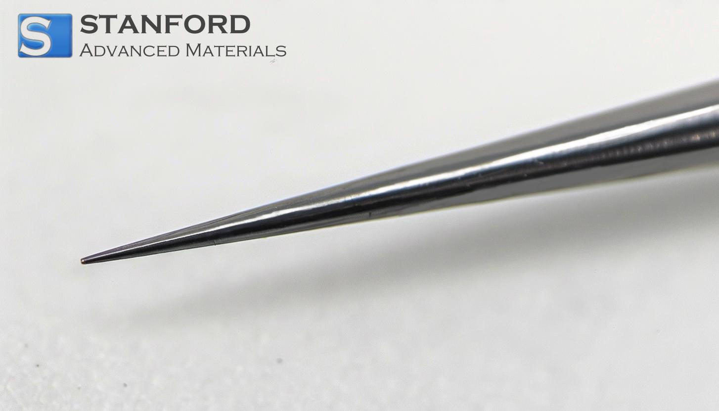
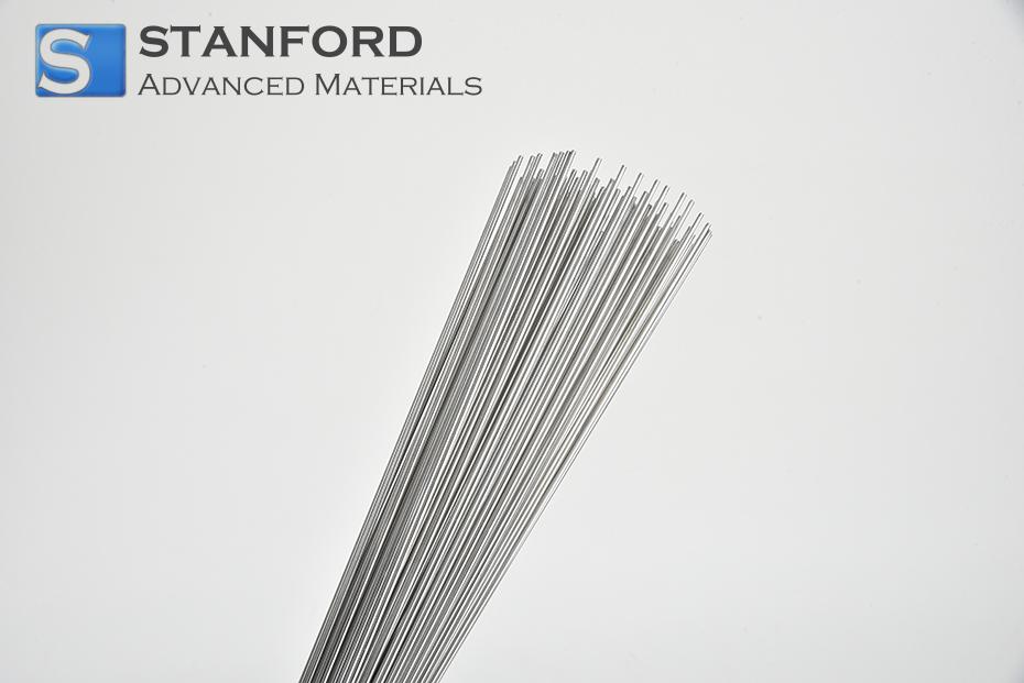
Palladium Alloy Probe Tip Description
Palladium Alloy Probe Tip is a precision-made component used in various high-precision applications, particularly in electronics, analytical testing, and industrial measurement systems. The tip is made from high-purity palladium, known for its excellent corrosion resistance, conductivity, and stability under high temperatures and harsh environments. Palladium Alloy Probe Tips are designed to provide consistent, reliable contact in electrical testing, semiconductor device probing, and chemical analysis.
Palladium Alloy Probe Tip Specification
|
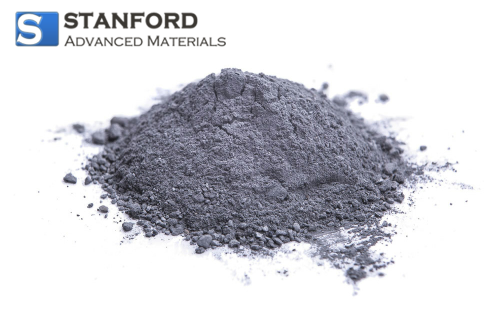
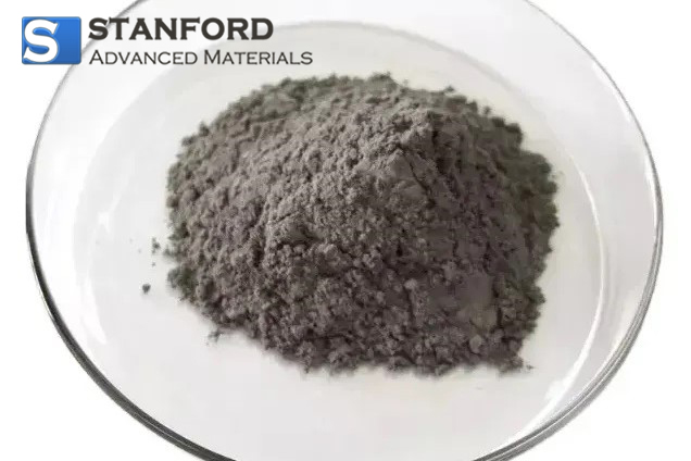
Material
|
Pd, Ag, Cu
|
|
Shape
|
tip
|
|
Tip Diameter
|
12μm
|
|
Shank Diameter
|
0.63mm
|
|
Length
|
19mm
|
|
Melting Point
|
1015℃
|
|
Chemical Composition (Theoretical)
|
Pd: 40±1%
Ag: 28.5±1%
Cu: Bal.
Or customized.
|
Palladium Alloy Probe Tip Application
- Semiconductor Testing: Used in probing systems for integrated circuit (IC) testing and device characterization.
- Electrical Probing: Ideal for high-frequency and high-precision electrical measurements, ensuring stable contact and minimal signal interference.
- Electrochemical Sensing: Palladium's ability to absorb hydrogen makes it useful in electrochemical sensors and fuel cell applications.
- Surface and Chemical Analysis: For applications like scanning probe microscopy (SPM) or atomic force microscopy (AFM), where fine, reliable contacts are essential.
- Industrial Measurements: In manufacturing environments for quality control, testing, and ensuring precise electrical measurements.
Palladium Alloy Probe Tip Packaging
Our Palladium Alloy Probe Tip is carefully handled during storage and transportation to preserve the quality of our product in its original condition. Packaged according to individual requirements
Tips are sold by the box including quantity of 5 tips.
FAQs
Q1: What is a Palladium Alloy Probe Tip (Pd-Ag-Cu)?
A Palladium Alloy Probe Tip (Pd-Ag-Cu) is a precision contact component made from a specialized alloy consisting of palladium (Pd), silver (Ag), and copper (Cu). This combination of metals provides the probe tip with excellent electrical conductivity, corrosion resistance, and strength, making it suitable for high-precision applications such as semiconductor testing and electrochemical sensing.
Q2: How does a Palladium Alloy Probe Tip perform in high-temperature environments?
Palladium Alloy Probe Tips perform well in high-temperature environments due to the thermal stability provided by the palladium and copper components. The probe tips maintain their integrity and performance even when exposed to elevated temperatures, making them suitable for use in demanding conditions such as testing high-temperature semiconductor devices.
Q3: Can Palladium Alloy Probe Tips be used for high-frequency electrical testing?
Yes, Palladium Alloy Probe Tips are ideal for high-frequency electrical testing due to their excellent electrical conductivity and low contact resistance. This ensures that the probe tip provides stable and reliable contact, which is essential for accurate high-frequency measurements, especially in semiconductor and electronics testing.