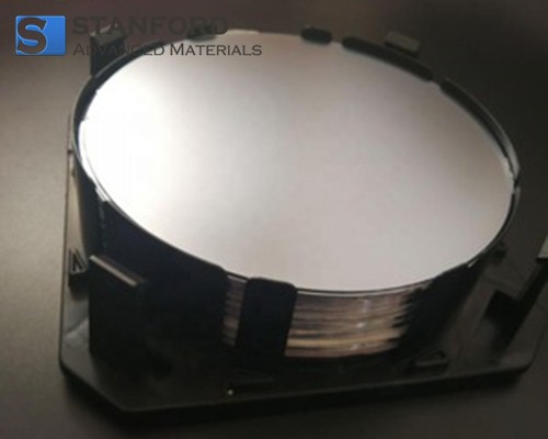
IN2270 Indium Antimonide Wafer
| Catalog No. | IN2270 |
| Material | InSb |
| Thickness | 500 um - 625 um |
| Conductive Type | N - type |
| Diameter | Ø 2" Ø 3" |
Stanford Advanced Materials (SAM) provides a wide range of compound wafers including GaAs wafers, GaP wafers, GaSb wafers, InAs wafers, and InP wafers.
Related products: Gallium Nitride Wafer, Gallium Arsenide Wafer, Germanium Wafer (Ge wafer), Gallium Phosphide Wafer, Indium Arsenide Wafer.
INQUIRY
Add to Inquiry List
Description
Specification
Description of Indium Antimonide Wafer
Indium antimonide (InSb) is a crystalline compound made from the elements indium (In) and antimony (Sb). It is a narrow-gap semiconductor material from the III-V group used in infrared detectors, including thermal imaging cameras, FLIR systems, infrared homing missile guidance systems, and infrared astronomy. The indium antimonide detectors are sensitive between 1–5 µm wavelengths. Indium antimonide was a very common detector in the old, single-detector mechanically scanned thermal imaging systems. Another application is as a terahertz radiation source as it is a strong photo-Dember emitter.
Specifications of Indium Antimonide Wafer
|
Growth |
LEC |
|
Diameter |
Ø 2" / Ø 3" |
|
Thickness |
500 um - 625 um |
|
Orientation |
(100)+/- 0.5° |
|
Off orientation |
Off 2° to 10° |
|
Surface |
One side polished or two sides polished |
|
Flat options |
EJ or SEMI. Std. |
|
Mobility |
(5.0-3.5)E5 cm2/Vs |
|
EPD |
<= 200 cm-2 |
|
Grade |
Epi polished grade / mechanical grade |
|
Package |
Single wafer container |
Applications of Indium Antimonide Wafer
- Solar photovoltaic
- Integrated circuits
- Transistor
LATEST RECOMMENDED
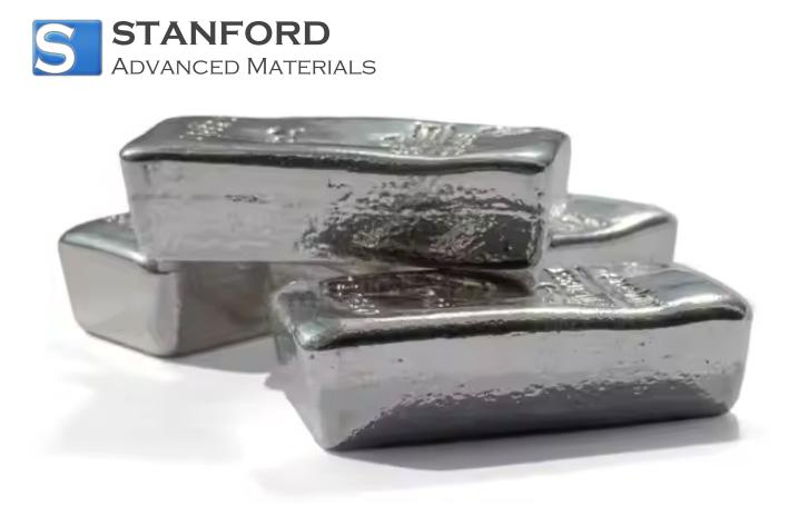
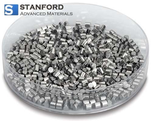
IN0480 Indium Ingot (In Ingot)
ITO0491 Indium Tin Oxide (ITO) Sputtering Targets
VD0554 Indium (In) Evaporation Materials
VD0623 Copper Indium (Cu/In) Evaporation Materials

VD0690 Indium Gallium Zinc Oxide (InGaZnOx) Evaporation Materials
VD0691 Indium Iron Oxide (InFe2O4) Evaporation Materials
VD0692 Indium Oxide (In2O3) Evaporation Materials
VD0693 Indium Tin Oxide (ITO) Evaporation Materials
GET A QUOTE
Send us an Inquiry now to find out more Information and the latest prices,thanks!