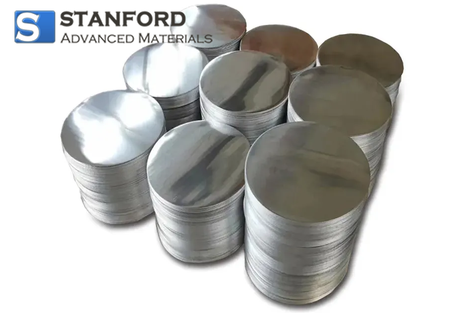
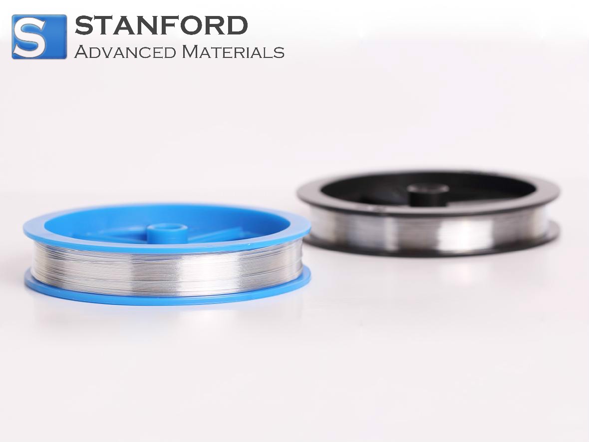
Aluminum Wafer Description:
Aluminum Wafers are thin slices of high-purity aluminum known for their versatility and essential role in semiconductor and electronics industries. With a face-centered cubic crystal structure and a lattice parameter of approximately 4.05 Å, they provide a stable substrate for the fabrication of electronic devices like integrated circuits and microchips. These wafers boast excellent thermal and electrical conductivity, crucial for efficient heat dissipation and signal transmission. Furthermore, their flat, smooth surface facilitates precise patterning and deposition processes during semiconductor manufacturing. Overall, Aluminum Wafers are indispensable components in the production of advanced electronic technologies.
Aluminum Wafer Specifications:
|
Melting Point
|
660.37℃
|
|
Boiling Point
|
2467℃
|
|
Density
|
2.7 g/cm3
|
|
Electrical Resistivity
|
2.6548 microhm-cm @ 0℃
|
|
Electronegativity
|
1.5 Paulings
|
|
Heat of Fusion
|
2.55 Cal/gm mole
|
|
Heat of Vaporization
|
67.9 K-Cal/gm at om at 765℃
|
|
Poisson's Ratio
|
0.35
|
|
Specific Heat
|
0.215 Cal/g/ K @ 25℃
|
|
Tensile Strength
|
6800 psi Coldroled 16,000 psi.
|
|
Thermal Conductivity
|
2.37 W/cm/ K @ 298.2 K
|
|
Thermal Expansion
|
(25℃) 23.1 µm·m-1·K-1
|
|
Vickers Hardness
|
167 MPa
|
|
Young's Modulus
|
70 GPa
|
Aluminum Wafer Applications:
1. Integrated Circuit Manufacturing: Aluminum Wafers play a key role in the manufacturing of integrated circuits (ICs) as substrates for semiconductor devices. They provide a flat, stable base on which to deposit and prepare the various layers of an IC.
2. Microelectronic Devices: Aluminum Wafers are used in the fabrication of a variety of microelectronic devices such as transistors, photodiodes, and solar cells. These devices usually require process steps such as doping, thin film deposition and microfabrication on Aluminum Wafers.
3. Sensor Fabrication: Aluminum Wafers are also used to fabricate a variety of sensors such as pressure sensors, temperature sensors, optical sensors, etc. These sensors usually require doping, thin film deposition and microfabrication on the wafer. These sensors usually require specific process treatments and assembly on the wafer surface to achieve specific sensing functions.
4. Optical applications: In some optical applications, Aluminum Wafers are used as substrates for optical components. They can be used as the basis for mirrors, refractors, optical filters, etc., and are used to prepare a variety of optical devices and systems.
5. Research and development: Aluminum Wafers are also widely used in research and development to study new materials, processes and methods of preparing new devices, and to advance semiconductor and electronic technology.
Aluminum Wafer Safety Information:
|
Symbol
|

|
|
Signal word
|
Warning
|
|
Hazard statements
|
H400
|
|
Precautionary statements
|
P273
|
|
Transport Information
|
UN 3077 9 / PGIII
|
|
WGK Germany
|
3
|